Diodes DMS3012SFG User Manual

30V N-CHANNEL ENHANCEMENT MODE MOSFET WITH SCHOTTKY DIODE
Product Summary
I
V
R
(BR)DSS
10m @ V
30V
15m @ VGS = 4.5V
Package
DS(ON)
= 10V
GS
POWERDI
3333-8
D
TA = +25°C
12A
9.5A
Description
This MOSFET has been designed to minimize the on-state resistance
(R
) and yet maintain superior switching performance, making it
DS(on)
ideal for high efficiency power management applications.
Applications
• Backlighting
• Power Management Functions
• DC-DC Converters
Top View
D
D
D
D
Bottom View
Pin 1
S
S
S
G
DMS3012SFG
POWERDI
Features
• DIOFET utilizes a unique patented process to monolithically
integrate a MOSFET and a Schottky in a single die to deliver:
Low R
Low V
Low Q
– minimize conduction losses
DS(ON)
– reducing the losses due to body diode conduction
SD
– lower Qrr of the integrated Schottky reduces body
rr
diode switching losses
Low gate capacitance (Q
) ratio – reduces risk of shoot
g/Qgs
through or cross conduction currents at high frequencies
• Small form factor thermally efficient package enables higher
density end products
• Occupies just 33% of the board area occupied by SO-8 enabling
smaller end product
• 100% UIS (Avalanche) rated
• 100% Rg tested
• Totally Lead-Free & Fully RoHS Compliant (Notes 1 & 2)
• Halogen and Antimony Free. “Green” Device (Note 3)
• Qualified to AEC-Q101 Standards for High Reliability
Mechanical Data
• Case: POWERDI3333-8
• Case Material: Molded Plastic, "Green" Molding Compound.
UL Flammability Classification Rating 94V-0
• Moisture Sensitivity: Level 1 per J-STD-020
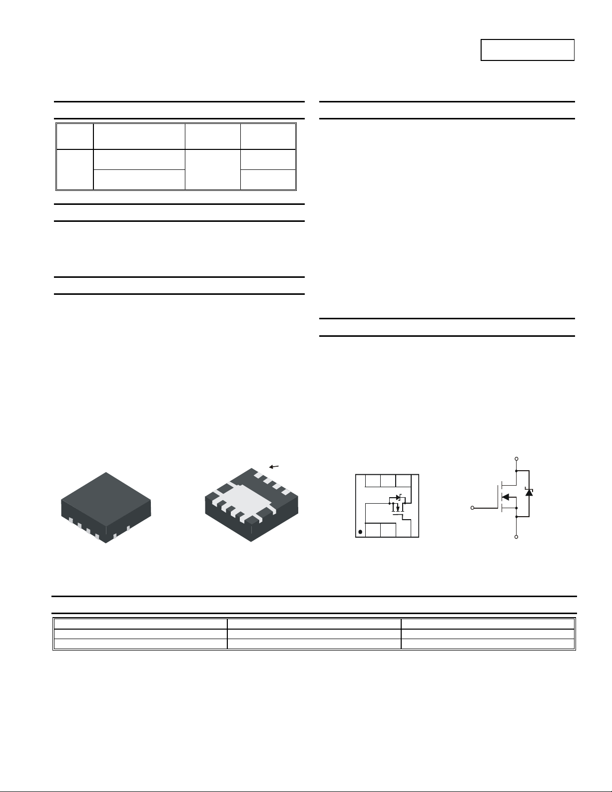
• Terminal Connections Indicator: See diagram
Terminals: Finish - Matte Tin annealed over Copper leadframe.
Solderable per MIL-STD-202, Method 208
• Weight: 0.072 grams (approximate)
Drain
8765
Gate
Source
234
1
Top View
Pin Configuration
Internal Schematic
®
Ordering Information (Note 4)
Part Number Case Packaging
DMS3012SFG-7 POWERDI3333-8 2000/Tape & Reel
DMS3012SFG-13 POWERDI3333-8 3000/Tape & Reel
Notes: 1. No purposely added lead. Fully EU Directive 2002/95/EC (RoHS) & 2011/65/EU (RoHS 2) compliant.
2. See http://www.diodes.com for more information about Diodes Incorporated’s definitions of Halogen- and Antimony-free, "Green" and Lead-free.
4. For packaging details, go to our website at http://www.diodes.com.
3. Halogen- and Antimony-free "Green” products are defined as those which contain <900ppm bromine, <900ppm chlorine (<1500ppm total Br + Cl) and
<1000ppm antimony compounds.
POWERDI is a registered trademark of Diodes Incorporated.
DMS3012SFG
Document number: DS35441 Rev. 7 - 2
1 of 8
www.diodes.com
October 2012
© Diodes Incorporated

θ
Marking Information
Maximum Ratings (@T
Drain-Source Voltage
Gate-Source Voltage
Continuous Drain Current (Note 6) VGS = 10V
Continuous Drain Current (Note 6) VGS = 4.5V
Pulsed Drain Current (10s pulse, duty cycle = 1%)
Maximum Continuous Body Diode Forward Current (Note 6)
Avalanche Current (Note 7) L = 0.1mH
Repetitive Avalanche Energy (Note 7) L = 0.1mH
YYWW
N12
= +25°C, unless otherwise specified.)
A
Characteristic Symbol Value Units
Steady
State
t < 10s
Steady
State
t < 10s
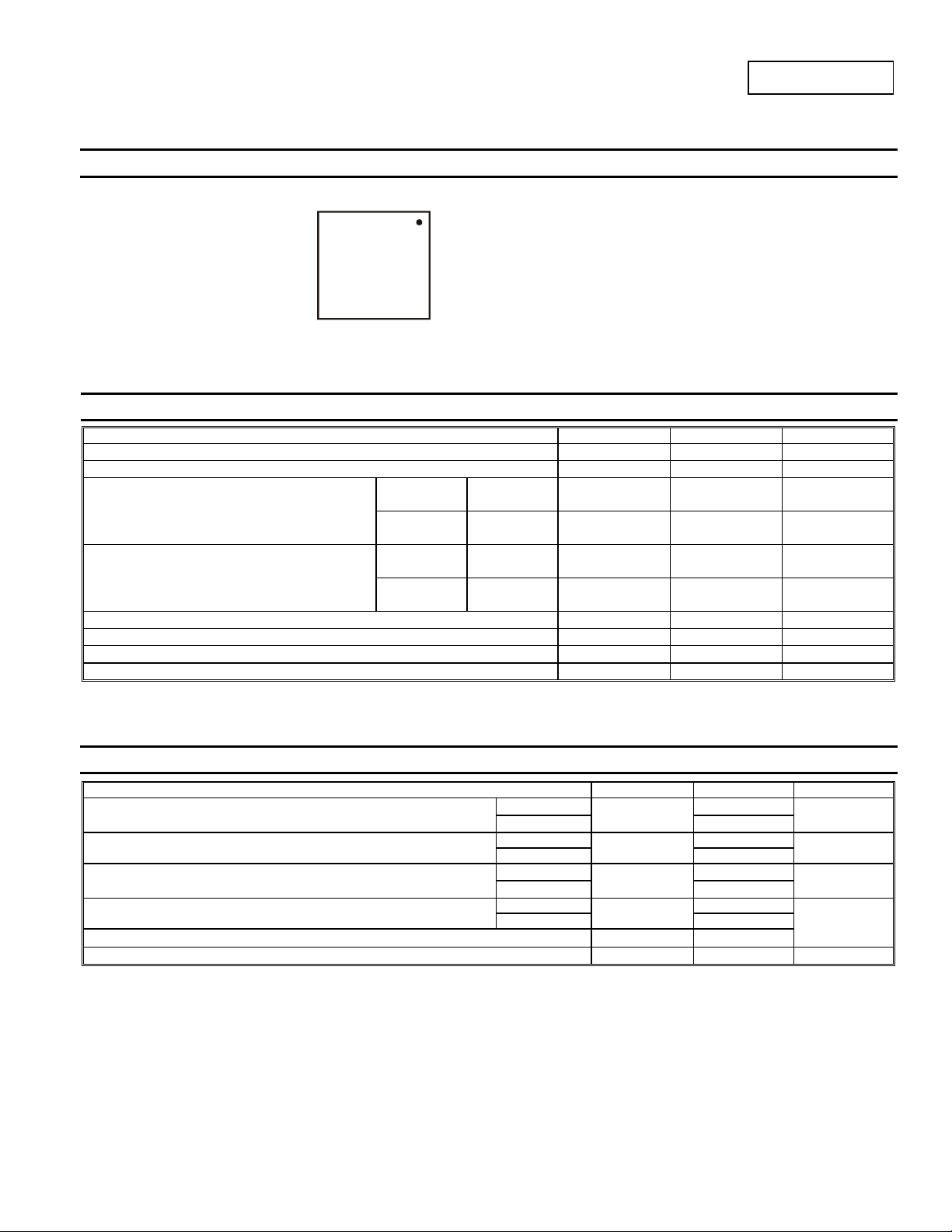
N12 = Product Type Marking Code
YYWW = Date Code Marking
YY = Last digit of year (ex: 11 = 2011)
WW = Week code (01 ~ 53)
V
DSS
V
GSS
T
= +25°C
A
T
= +70°C
A
= +25°C
T
A
= +70°C
T
A
T
= +25°C
A
T
= +70°C
A
= +25°C
T
A
= +70°C
T
A
I
D
I
D
I
D
I
D
I
DM
I
S
I
AR
E
AR
DMS3012SFG
30 V
±20 V
12
9.5
16.0
12.7
9.5
7.5
13.0
10.3
90 A
3.5 A
17 A
43 mJ
A
A
A
A
Thermal Characteristics
Characteristic Symbol Value Units
T
= +25°C
Total Power Dissipation (Note 5)
Thermal Resistance, Junction to Ambient (Note 5)
Total Power Dissipation (Note 6)
Thermal Resistance, Junction to Ambient (Note 6)
Thermal Resistance, Junction to Case (Note 6)
Operating and Storage Temperature Range
Notes: 5. Device mounted on FR-4 substrate PC board, 2oz copper, with minimum recommended pad layout.
6. Device mounted on FR-4 substrate PC board, 2oz copper, with 1inch square copper plate.
7. I
and EAR rating are based on low frequency and duty cycles to keep TJ = +25°C
AR
A
TA = +70°C
Steady state
t < 10s 74
= +25°C
T
A
TA = +70°C
Steady State
t < 10s 31
P
R
P
R
R
T
J, TSTG
D
JA
θ
D
JA
θ
JC
POWERDI is a registered trademark of Diodes Incorporated.
DMS3012SFG
Document number: DS35441 Rev. 7 - 2
2 of 8
www.diodes.com
0.89
0.55
145
2.2
1.3
W
°C/W
W
58
°C/W
11
-55 to +150 °C
October 2012
© Diodes Incorporated

RAIN CUR
R
N
T
P
P
T
R
T P
O
R
T
R
T T
HER
R
TANC
DMS3012SFG
(A)
E
-I , D
100
D
10
1
0.1
100
(W)
IWE
ANSIEN
EAK
,
(PK)
90
80
70
60
50
40
30
20
Single Pulse
°
R = 61C/W
θ
JA
R = r * R
θθ
JA(t) (t) JA
T - T = P * R
JA JA(t)
θ
10
0.01
0.1 1 10 100
-V , DRAIN-SOURCE VOL TAGE (V)
DS
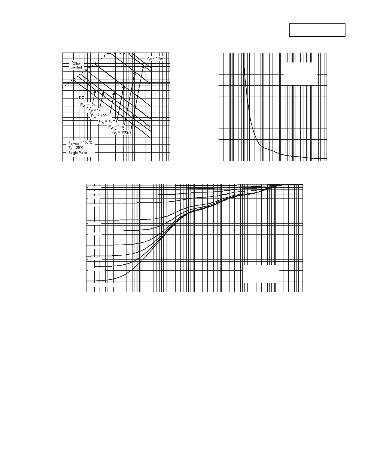
Fig. 1 SOA, Safe Opera t ion Area
1
D = 0.9
D = 0.7
E
D = 0.5
D = 0.3
0
0.001 0.01 0.1 1 10 100 1,000
0.0001
t1, PULSE DURATION TIME (sec)
Fig. 2 Single Pulse Maximum Power Dissipation
ESIS
0.1
D = 0.1
MAL
D = 0.05
D = 0.02
0.01
D = 0.01
ANSIEN
D = 0.005
r(t),
D = Single Pulse
0.001
0.00001 0.0001 0.001 0.01 0.1 1 10 100 1,000
R = r * R
θ
JA(t) (t)
R = 61C/W
JA
Duty Cycle, D = t1/t2
θθJA
°
t1, PULSE DURATION TIME (sec)
Fig. 3 Transient Therma l R esistan ce
POWERDI is a registered trademark of Diodes Incorporated.
DMS3012SFG
Document number: DS35441 Rev. 7 - 2
3 of 8
www.diodes.com
October 2012
© Diodes Incorporated
 Loading...