

Page 1
Features
• Low On-Resistance
• 95mΩ @V
• 120mΩ @V
• 150mΩ (typ) @V
• Low Gate Threshold Voltage, -1.3V Max
• Fast Switching Speed
• Low Input/Output Leakage
• Incorporates Low V
• Low Profile, 0.5mm Max Height
• Totally Lead-Free & Fully RoHS Compliant (Notes 1 & 2)
• Halogen and Antimony Free. “Green” Device (Note 3)
• Qualified to AEC-Q101 Standards for High Reliability
NEW PRODUCT
= -4.5V
GS
= -2.5V
GS
= -1.8V
GS
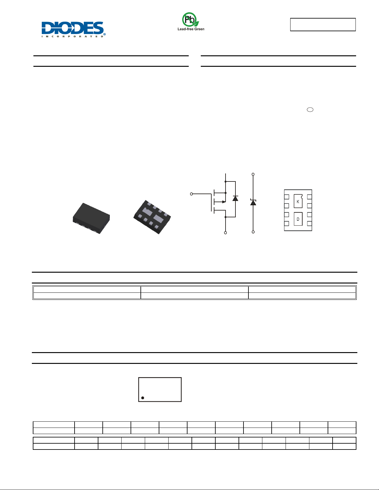
Super Barrier Rectifier (SBR)
F
U-DFN3020-8
Type B
Top View
Bottom View
DMS2120LFWB
P-CHANNEL ENHANCEMENT MODE MOSFET WITH INTEGRATED SBR
SUPER BARRIER RECTIFIER
Mechanical Data
• Case: U-DFN3020-8 Type B
• Case Material: Molded Plastic, “Green” Molding Compound. UL
Flammability Classification Rating 94V-0
• Moisture Sensitivity: Level 1 per J-STD-020
• Terminal Connections: See Diagram
• Terminals: Finish – NiPdAu annealed over Copper leadframe.
Solderable per MIL-STD-202, Method 208
• Weight: 0.011 grams (approximate)
S
G
D
Equivalent Circuit
K
K
K
D
D
A
Bottom View
e4
A
A
S
G
®
Ordering Information (Note 4)
Part Number Case Packaging
DMS2120LFWB-7 DFN3020B-8 3000/Tape & Reel
Notes: 1. No purposely added lead. Fully EU Directive 2002/95/EC (RoHS) & 2011/65/EU (RoHS 2) compliant.
2. See http://www.diodes.com for more information about Diodes Incorporated’s definitions of Halogen- and Antimony-free, "Green" and Lead-free.
3. Halogen- and Antimony-free "Green” products are defined as those which contain <900ppm bromine, <900ppm chlorine (<1500ppm total Br + Cl) and
<1000ppm antimony compounds.
4. For packaging details, go to our website at http://www.diodes.com.
Marking Information
Date Code Key
Year 2008 2009 2010 2011 2012 2013 2014 2015 2016 2017
Code V W X Y Z A B C D E
Month Jan Feb Mar Apr May Jun Jul Aug Sep Oct Nov Dec
Code 1 2 3 4 5 6 7 8 9 O N D
SBR is a registered trademark of Diodes Incorporated.
MF
YM
DMS2120LFWB
Document number: DS31667 Rev. 5 - 2
MF = Product Type Marking Code
YM = Date Code Marking
Y = Year (ex: V = 2008)
M = Month (ex: 9 = September)
1 of 7
www.diodes.com
September 2012
© Diodes Incorporated
Page 2
θ
)
)
(BR)
Maximum Ratings – TOTAL DEVICE (@T
= +25°C, unless otherwise specified.)
A
Characteristic Symbol Value Unit
Power Dissipation (Note 5)
Thermal Resistance, Junction to Ambient
Operating and Storage Temperature Range
Maximum Ratings – P-CHANNEL MOSFET – Q1 (@T
Characteristic Symbol Value Units
Drain-Source Voltage
Gate-Source Voltage
Drain Current (Note 5)
Pulsed Drain Current (Note 6)
NEW PRODUCT
Maximum Ratings – SBR – D1 (@T
Characteristic Symbol Value Unit
Peak Repetitive Reverse Voltage
Working Peak Reverse Voltage
DC Blocking Voltage
RMS Reverse Voltage
Average Rectified Output Current
Non-Repetitive Peak Forward Surge Current
8.3ms single half sine-wave superimposed on rated load
= +25°C, unless otherwise specified.)
A
P
D
R
JA
T
, T
J
STG
= +25°C, unless otherwise specified.)
A
V
DSS
V
GSS
I
D
I
DM
V
RRM
V
RWM
V
R
V
R(RMS
I
O
I
FSM
1.5 W
85
-55 to +150
-20 V
±12 V
-2.9 A
-10 A
20 V
14 V
1 A
3 A
DMS2120LFWB
°C/W
°C
Electrical Characteristics – P-CHANNEL MOSFET – Q1 (@T
= +25°C, unless otherwise specified.)
A
Characteristic Symbol Min Typ Max Unit Test Condition
OFF CHARACTERISTICS (Note 7)
Drain-Source Breakdown Voltage
Zero Gate Voltage Drain Current
Gate-Source Leakage
BV
I
DSS
I
GSS
-20
DSS
⎯ ⎯
⎯ ⎯ ⎯
⎯ ⎯
-1
±100
±800
⎯
V
VGS = 0V, ID = -250μA
μA
VDS = -20V, VGS = 0V
= ±8V, VDS = 0V
V
GS
nA
V
= ±12V, VDS = 0V
GS
ON CHARACTERISTICS (Note 7)
Gate Threshold Voltage
Static Drain-Source On-Resistance
Forward Transfer Admittance
Diode Forward Voltage (Note 7)
V
R
DS (ON)
|Y
V
GS(th
| ⎯
fs
⎯
SD
-0.45
⎯
⎯
⎯
-1.3 V
⎯
70
95
84
120
150
⎯
mΩ
S
100
8
0.42 -1.2 V
VDS = VGS, ID = -250μA
V
= -4.5V, ID = -2.8A
GS
VGS = -2.5V, ID = -2.0A
VGS = -1.8V, ID = -1.0A
VDS = -5V, ID = -2.8A
VGS = 0V, IS = -1.0A
DYNAMIC CHARACTERISTICS
Input Capacitance
Output Capacitance
Reverse Transfer Capacitance
C
iss
C
oss
C
rss
⎯
⎯
⎯
632
65
54
⎯
⎯
⎯
pF
pF
pF
V
= -10V, VGS = 0V
DS
f = 1.0MHz
Electrical Characteristics – SBR – D1 (@T
= +25°C, unless otherwise specified.)
A
Characteristic Symbol Min Typ Max Unit Test Condition
Reverse Breakdown Voltage (Note 7)
Forward Voltage
V
V
Reverse Current (Note 7)
Notes: 5. Device mounted on FR-4 PCB, on minimum recommended, 2oz Copper pad layout.
7. Short duration pulse test used to minimize self-heating effect.
6. Repetitive rating, pulse width limited by junction temperature.
20
R
⎯
F
⎯ ⎯ ⎯
I
⎯ ⎯
R
⎯ ⎯
0.45
0.52
80
V
V
μA
IR = 1mA
= 0.5A
I
F
I
= 1.0A
F
VR = 20V
SBR is a registered trademark of Diodes Incorporated.
DMS2120LFWB
Document number: DS31667 Rev. 5 - 2
2 of 7
www.diodes.com
September 2012
© Diodes Incorporated
Page 3
RAIN
CUR
REN
T
R
CUR
RENT
R
RAIN-SOUR
CE O
N-R
TAN
C
R
RAIN-SOUR
CE O
N-R
TAN
C
R
R
OUR
C
NEW PRODUCT
DMS2120LFWB
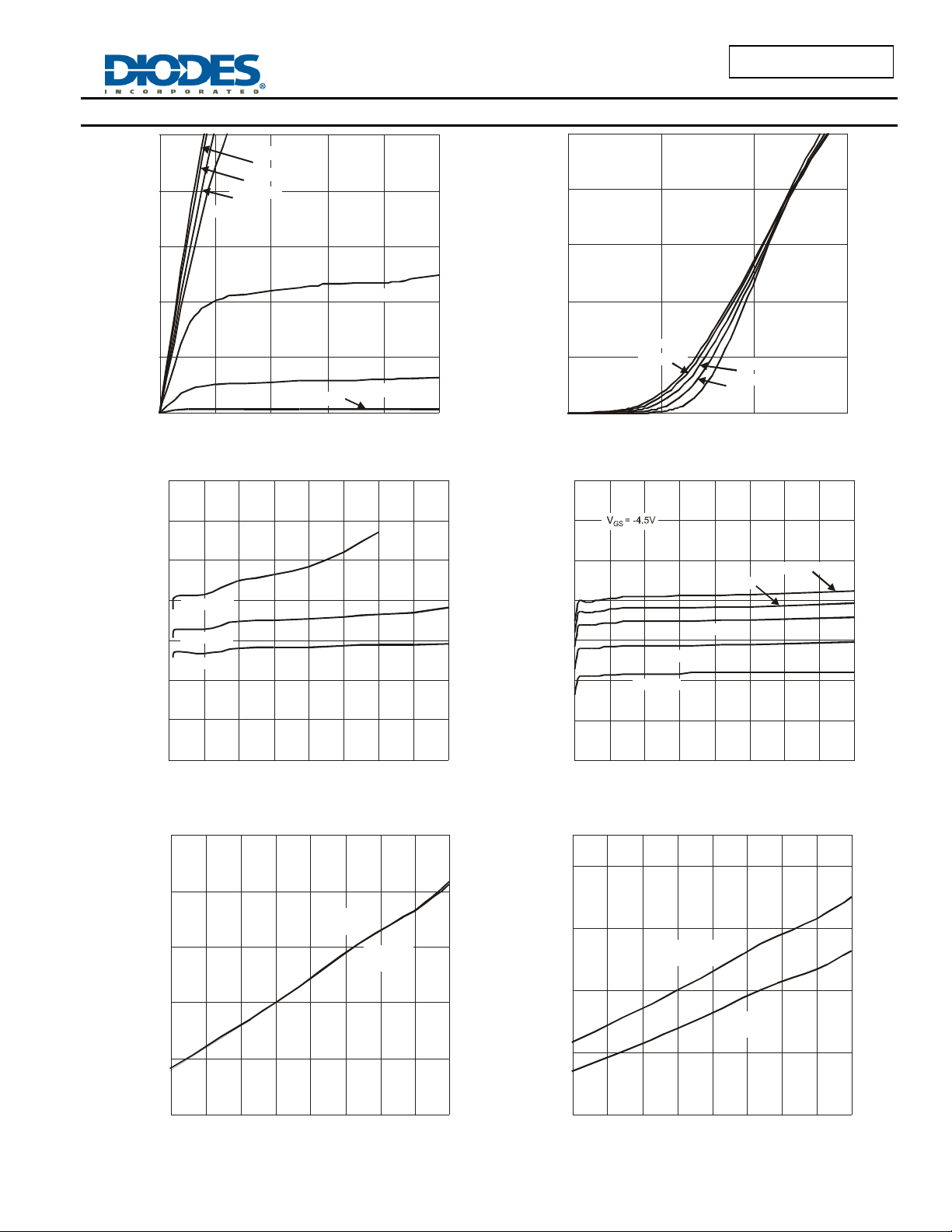
Q1, P-CHANNEL MOSFET
10
8
(A)
V = -8.0V
GS
V = -4.5V
GS
V = -2.5V
GS
V = -2.0V
GS
6
-I , D
4
D
V = -1.5V
GS
2
V = -1.2V
V = -1.0V
0
01 2 3 45
-V , DRAIN-SOURCE VOLTAGE (V)
DS
GS
GS
Fig. 1 Typical Output C har acteristic s
0.14
Ω
E ( )
0.12
10
V = -5V
DS
8
(A)
6
AIN
4
D
-I , D
2
0
T = 150°C
A
T = 125°C
A
T = 25°C
A
T = -55°C
A
T = 85°C
A
0.5 1 1.5 2
-V , GATE SOURCE VOLTAGE (V)
GS
Fig. 2 Typical Transfer Characteristics
0.14
Ω
E ( )
0.12
0.1
ESIS
0.08
V = -1.8V
GS
V = -2.5V
0.06
GS
V = -4.5V
GS
0.04
, D
0.02
DS(ON)
0
012345678
-I , DRAIN CURRENT (A)
D
Fig. 3 Typical On-Resistance
vs. Drain C urrent and G ate V ol tage
1.6
1.4
E
AIN-S
, D
DS(ON)
1.2
1.0
0.8
ON-RESISTA NCE (NORMA LIZED)
V = -2.5V
GS
I = -2A
D
V = -4.5V
GS
I = -5A
D
0.1
ESIS
T = 125°C
A
T = 150°C
A
0.08
T = 85°C
0.06
0.04
T = -55°C
A
T = 25°C
A
A
, D
0.02
DS(ON)
0
01234 5678
-I , DRAIN CURRENT (A)
D
Fig. 4 Typical Drain-Source On-Resistance
vs. Drain C urrent and Temperature
Ω
0.11
0.09
V = -2.5V
GS
I = -2A
D
0.07
V = -4.5V
GS
I = -5A
D
0.05
0.6
-50 -25 0 25 50 75 100 125 150
T , JUNCTION TEMPERATURE (°C)
J
Fig. 5 On-Resistance Variation with T emperature
SBR is a registered trademark of Diodes Incorporated.
DMS2120LFWB
Document number: DS31667 Rev. 5 - 2
3 of 7
www.diodes.com
DS(ON)
0.03
R , DRAIN-SOURCE ON-RESISTANCE ( )
-50 -25 0 25 50 75 100 125 150
T , JUNCTION TEMPERA TURE (°C)
J
Fig. 6 On-Resistance Variation with Temperature
September 2012
© Diodes Incorporated
Page 4

C, CAPACIT
C
F
GAT
T
H
RESH
O
O
TAG
OUR
CE CUR
RENT
NEW PRODUCT
DMS2120LFWB
10,000
f = 1MHz
)
1,000
E (p
AN
100
C
iss
C
oss
C
rss
10
048121620
-V , DRAIN-SOURCE VOLTAGE (V)
DS
Fig. 7 Typical Capacitance
10
1
0.9
E (V)
0.8
L
0.7
LD V
0.6
0.5
E
I = -250µA
D
I = -1mA
D
0.4
0.3
GS(TH)
-V ,
0.2
-50 -25 0 25 50 75 100 125 150
T , AMBIENT TEMPERATURE (°C)
A
Fig. 8 Gate Threshold Variation vs. Ambient Temperature
8
(A)
6
T = 25°C
A
4
S
-I , S
2
0
0 0.2 0.4 0.6 0.8 1 1.2 1.4 1.6
-V , SOURCE-DRAIN VOLTAGE (V)
SD
Fig. 9 Diode Forward Voltage vs. Current
SBR is a registered trademark of Diodes Incorporated.
DMS2120LFWB
Document number: DS31667 Rev. 5 - 2
4 of 7
www.diodes.com
September 2012
© Diodes Incorporated
Page 5

P, P
OWER
PATIO
N
C, CAPACITAN
C
F
NEW PRODUCT
DMS2120LFWB
D1, SBR
0.7
0.6
(W)
0.5
0.4
DISSI
0.3
0.2
D
0.1
0
0 0.5 1 1.5
I , AVERAGE FORWARD CURRENT (A)
F(AV)
Fig. 10 Forward Power Dissipation
10,000
1
T = 150°C
A
T = 125°C
0.1
A
T = 85°C
A
T = 25°C
A
T = -55°C
A
0.001
F
I , INST ANTANEOUS FORWARD CURRENT (A)
0.0001
0.01
0 0.1 0.2 0.3 0.4 0.5 0.6 0.7
V , INSTANTANEOUS FORWARD VOLTAGE (V)
F
Fig. 11 Typical Forw ar d Charact er istics
10,000
0.8
T = 150°C
1,000
100
A
T = 125°C
A
T = 85°C
A
10
1
T = 25°C
A
0.1
R
0.01
I , INSTANTANEOUS REVERSE CURRENT(uA)
0 5 10 15 20 25 30 35 40
V , INSTANTANEOUS REVERSE VOLTAGE (V)
R
Fig. 12 Typical Reverse Characteristics
1.6
1.4
1.2
Note 5
1.0
0.8
)
1,000
f = 1MHz
E (p
100
10
1
0.1 1 10 100
V , DC REVERSE VOLTAGE (V)
R
Fig. 13 T otal Capacitance vs. Reverse Voltage
150
125
100
75
0.6
50
0.4
25
0.2
F(AV)
I , AVERAGE FORWARD CURRENT (A)
0
25 50 75 100 125 150 175
T , AMBIENT TEMPERATURE (°C)
A
Fig. 14 Forward Current Derating Curve
SBR is a registered trademark of Diodes Incorporated.
DMS2120LFWB
Document number: DS31667 Rev. 5 - 2
5 of 7
www.diodes.com
A
T , DERA TED AMBIENT TEMPERATURE (°C)
0
010203040
V , DC REVERSE VOLTAGE (V)
R
Fig. 15 Operating Temperature Derating
September 2012
© Diodes Incorporated
Page 6

Package Outline Dimensions
Please see AP02002 at http://www.diodes.com/datasheets/ap02002.pdf for latest version.
NEW PRODUCT
A
A1
D
D4 D4
E
L
D2
b
Z
E2
e
A3
Suggested Pad Layout
Please see AP02001 at http://www.diodes.com/datasheets/ap02001.pdf for the latest version.
G
C
b
X1
Dimensions
Y1
a
Y2
X2
DMS2120LFWB
U-DFN3020-8
Type B
Dim Min Max Typ
A 0.77 0.83 0.80
A1 0 0.05 0.02
A3 - - 0.15
b 0.25 0.35 0.30
D 2.95 3.075 3.00
D2 0.82 1.02 0.92
D4 1.01 1.21 1.11
e - - 0.65
E 1.95 2.075 2.00
E2 0.43 0.63 0.53
L 0.25 0.35 0.30
Z - - 0.375
All Dimensions in mm
Value (in mm)
a 0.09
b 0.365
C 0.65
G 0.285
X1 0.4
X2 1.12
Y1 0.5
Y2 0.73
SBR is a registered trademark of Diodes Incorporated.
DMS2120LFWB
Document number: DS31667 Rev. 5 - 2
6 of 7
www.diodes.com
September 2012
© Diodes Incorporated
Page 7

DIODES INCORPORATED MAKES NO WARRANTY OF ANY KIND, EXPRESS OR IMPLIED, WITH REGARDS TO THIS DOCUMENT,
INCLUDING, BUT NOT LIMITED TO, THE IMPLIED WARRANTIES OF MERCHANTABILITY AND FITNESS FOR A PARTICULAR PURPOSE
(AND THEIR EQUIVALENTS UNDER THE LAWS OF ANY JURISDICTION).
Diodes Incorporated and its subsidiaries reserve the right to make modifications, enhancements, improvements, corrections or other changes
without further notice to this document and any product described herein. Diodes Incorporated does not assume any liability arising out of the
application or use of this document or any product described herein; neither does Diodes Incorporated convey any license under its patent or
trademark rights, nor the rights of others. Any Customer or user of this document o r products described herein in such applica tions shall assume
all risks of such use and will agree to hold Diodes Incorporated and all the companies whose products are represented on Diodes Incorporated
website, harmless against all damages.
Diodes Incorporated does not warrant or accept any liability whatsoever in respect of any products purchased through unauthorized sales channel.
Should Customers purchase or use Diodes Incorporated products for any unintended or unauthorize d application, Customers shall indemnify and
NEW PRODUCT
hold Diodes Incorporated and its representatives harmless against all claims, damages, expenses, and attorney fees arising out of, directly or
indirectly, any claim of personal injury or death associated with such unintended or unauthorized application.
Products described herein may be covered by one or more United States, international or foreign patents pending. Product names and markings
noted herein may also be covered by one or more United States, international or foreign trademarks.
Diodes Incorporated products are specifically not authorized for use as critical components in life support devices or systems without the express
written approval of the Chief Executive Officer of Diodes Incorporated. As used herein:
A. Life support devices or systems are devices or systems which:
1. are intended to implant into the body, or
labeling can be reasonably expected to result in significant injury to the user.
B. A critical component is any component in a life support device or system whose failure to perform can be reasonably expected to cause the
failure of the life support device or to affect its safety or effectiveness.
Customers represent that they have all necessary expertise in the safety and regulatory ramifications of their life support devices or systems, and
acknowledge and agree that they are solely responsible for all legal, regulatory and safety-related requirements concerning their products and any
use of Diodes Incorporated products in such safety-critical, life support devices or systems, notwithstanding any devices- or systems-related
information or support that may be provided by Diodes Incorporated. Further, Customers must fully indemnify Diodes Incorporated and its
representatives against any damages arising out of the use of Diodes Incorporated products in such safety-critical, life support devices or systems.
Copyright © 2012, Diodes Incorporated
www.diodes.com
2. support or sustain life and whose failure to perform when properly used in accordance with instructions for use provided in th e
IMPORTANT NOTICE
LIFE SUPPORT
DMS2120LFWB
SBR is a registered trademark of Diodes Incorporated.
DMS2120LFWB
Document number: DS31667 Rev. 5 - 2
7 of 7
www.diodes.com
September 2012
© Diodes Incorporated
 Loading...