

Page 1
A
f
Product Summary
V
R
(BR)DSS
-40V
25mΩ @ V
45mΩ @ VGS = -4.5V
DS(on)
max
= -10V
GS
Description and Applications
This MOSFET has been designed to minimize the on-state resistance
and yet maintain superior switching performance, making it ideal for
high efficiency power management applications.
ADVANCE INFORMATION
• Motor control
• Backlighting
• DC-DC Converters
• Printer equipment
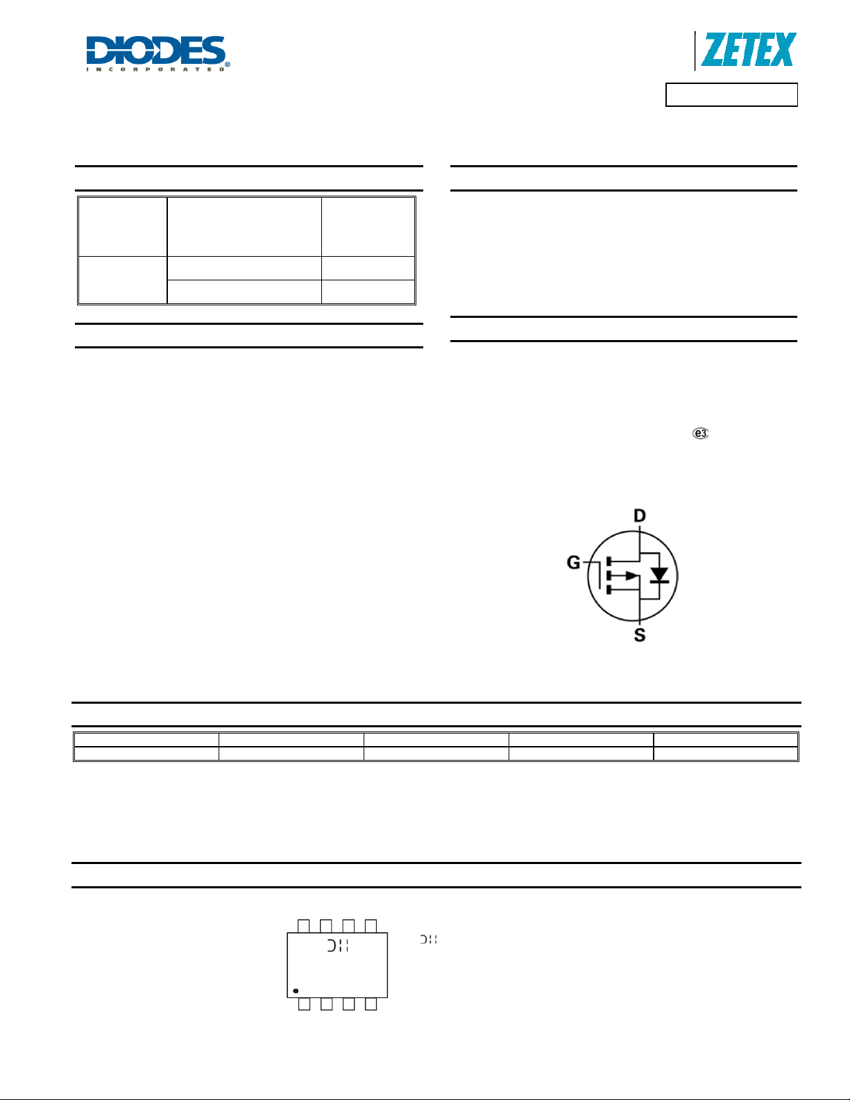
SO-8
Top View
Diodes Incorporated
40V P-CHANNEL ENHANCEMENT MODE MOSFET
Features and Benefits
max (A)
I
D
T
= 25°C
A
(Notes 6)
-8.0
-6.0
• Low R
• Fast switching speed – Minimizes switching losses
• Totally Lead-Free & Fully RoHS compliant (Notes 1 & 2)
• Halogen and Antimony Free. “Green” Device (Note 3)
• Qualified to AEC-Q101 Standards for High Reliability
– Minimizes conduction losses
DS(on)
Mechanical Data
• Case: SO-8
• Case Material: Molded Plastic, “Green” Molding Compound. UL
Flammability Classification Rating 94V-0 (Note 1)
• Moisture Sensitivity: Level 1 per J-STD-020
• Terminals: Finish - Matte Tin annealed over Copper lead frame.
Solderable per MIL-STD-202, Method 208
• Weight: 0.074 grams (approximate)
Pin-Out Top View Device symbol
Product Line o
DMP4025LSS
Ordering Information (Note 4)
Product Marking Reel size (inches) Tape width (mm) Quantity per reel
DMP4025LSS-13 P4025LS 13 12 2,500
Notes: 1. No purposely added lead. Fully EU Directive 2002/95/EC (RoHS) & 2011/65/EU (RoHS 2) compliant.
3. Halogen and Antimony free "Green” products are defined as those which contain <900ppm bromine, <900ppm chlorine (<1500ppm total Br + Cl) and
4. For packaging details, go to our website at http://www.diodes.com
2. See http://www.diodes.com for more info rmation about Diodes Incorporated’s definitions of Halogen and Antimony free,"Green" and Lead-Free.
<1000ppm antimony compounds.
Marking Information
DMP4025LSD
Document Number: DS35936 Rev: 1 - 2
P4025LS
YY WW
www.diodes.com
= Manufacturer’s Marking
P4025LS = Product Type Marking Code
YYWW = Date Code Marking
YY = Year (ex: 10 = 2010)
WW = Week (01 - 53)
1 of 8
June 2012
© Diodes Incorporated
Page 2
A
f
Product Line o
Diodes Incorporated
DMP4025LSS
Maximum Ratings @T
Drain-Source Voltage
Gate-Source Voltage
Continuous Drain Current
Pulsed Drain Current
Continuous Source Current (Body diode) (Notes 7)
Pulsed Source Current (Body diode) (Notes 7)
Thermal Characteristics @T
ADVANCE INFORMATION
Power Dissipation
Thermal Resistance, Junction to Ambient
Thermal Resistance, Junction to Lead (Notes 8)
Operating and Storage Temperature Range
Notes: 5. For a device surface mounted on minimum recommended FR4 PCB with high coverage of single sided 1oz copper, in still air conditions; the device is
measured when operating in a steady-state condition.
6. Same as note (2), except the device is surface mounted on 25mm X 25mm X 1.6mm FR4 PCB.
7. Repetitive rating on 25mm X 25mm FR4 PCB, D=0.02, pulse width 300µs – pulse width by maximum junction temperature.
8. Thermal resistance from junction to solder-point (at the end of the drain lead).
= 25°C unless otherwise specified
A
Characteristic Symbol Value Units
V
DSS
V
(Notes 6)
= -10V
V
GS
V
= -10V
GS
Characteristic Symbol Value Unit
TA = 70°C (Notes 6)
(Notes 5) -6.0
(Notes 7)
= 25°C unless otherwise specified
A
(Notes 5)
(Notes 6) 2.4
(Notes 5)
(Notes 6) 52
GSS
ID
IDM
I
I
SM
P
R
R
T
J, TSTG
S
θJA
θJL
D
-40
±20
-8.0
-6.9
-30
-8.0
-30
1.52
82
48.85
-55 to +150 °C
V
A
W
°C/W
DMP4025LSD
Document Number: DS35936 Rev: 1 - 2
2 of 8
www.diodes.com
June 2012
© Diodes Incorporated
Page 3
A
f
P
P
T
R
T P
O
R
T
R
T T
HER
R
TANC
Thermal Characteristics
ADVANCE INFORMATION
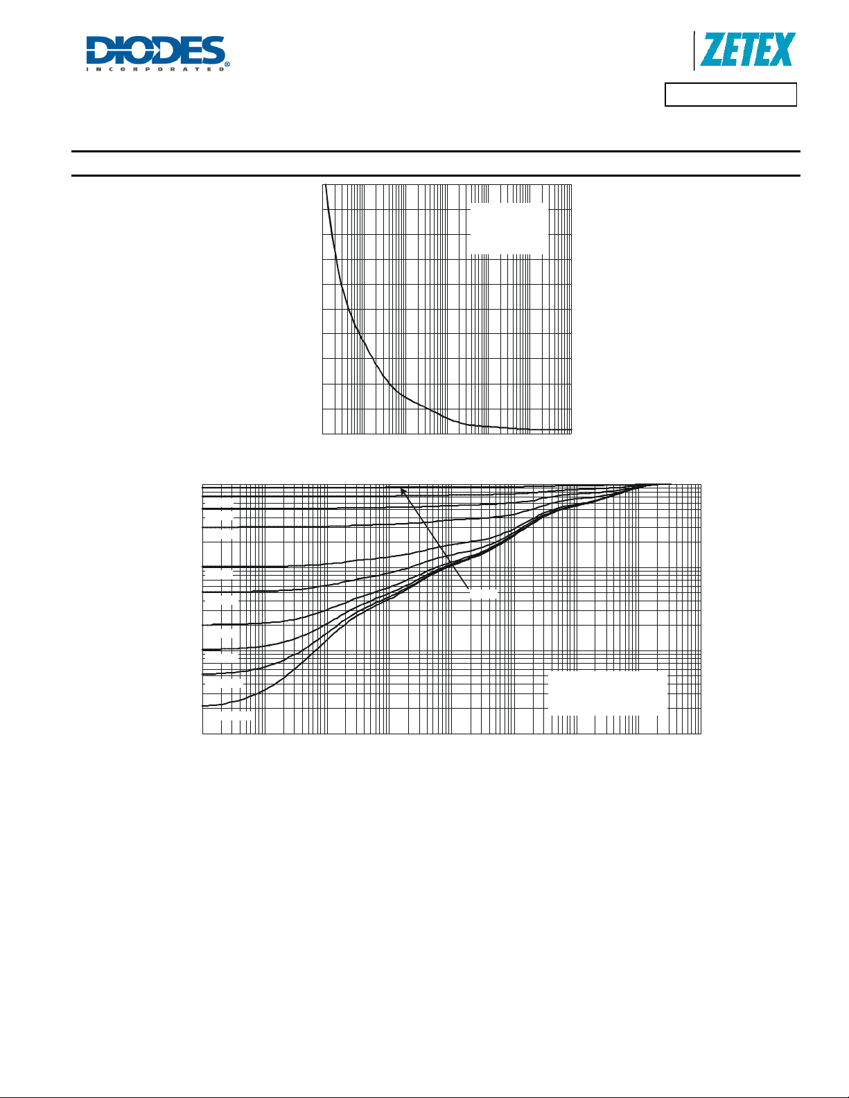
100
Single Pulse
°
R = 82C/W
θ
JA
R = r * R
θθ
JA(t) (t) JA
T - T = P * R
JA JA(t)
θ
(W)
IWE
90
80
70
60
50
ANSIEN
40
30
EAK
,
20
(PK)
10
0
0.001 0.01 0.1 1 10 100 1,000
t1, PULSE DURATION TIME (sec)
Fig. 1 Single Pulse Maximum Power Dissipation
Product Line o
Diodes Incorporated
DMP4025LSS
1
D = 0.7
E
D = 0.5
D = 0.3
ESIS
0.1
D = 0.1
MAL
D = 0.05
D = 0.02
0.01
D = 0.01
ANSIEN
D = 0.005
r(t),
Single Pulse
0.001
0.00001 0.0001 0.001 0.01 0.1 1 10 100 1,000
D = 0.9
R (t) = r(t) * R
θθ
JA JA
R = 83°C/W
θ
JA
Duty Cycle, D = t1/ t2
t1, PULSE DURATION TIMES (sec)
Fig. 2 Transi ent Thermal Resistance
DMP4025LSD
Document Number: DS35936 Rev: 1 - 2
3 of 8
www.diodes.com
June 2012
© Diodes Incorporated
Page 4

A
f
)
g
g
g
g
)
r
)
R
C
URR
T
R
CUR
RENT
Product Line o
Diodes Incorporated
DMP4025LSS
Electrical Characteristics T
= 25°C unless otherwise specified
A
Characteristic Symbol Min Typ Max Unit Test Condition
OFF CHARACTERISTICS
Drain-Source Breakdown Voltage
BV
Zero Gate Voltage Drain Current
Gate-Source Leakage
ON CHARACTERISTICS
Gate Threshold Voltage
Static Drain-Source On-Resistance (Note 9)
V
R
Forward Transconductance (Notes 9 & 10)
Diode Forward Voltage (Note 9)
DYNAMIC CHARACTERISTICS (Note 10)
Input Capacitance
Output Capacitance
Reverse Transfer Capacitance
ADVANCE INFORMATION
Gate Resistance Rg
Total Gate Charge (Note 11)
Total Gate Charge (Note 11)
Gate-Source Charge (Note 11)
Gate-Drain Charge (Note 11)
Turn-On Delay Time (Note 11)
Turn-On Rise Time (Note 11)
Turn-Off Delay Time (Note 11)
Turn-Off Fall Time (Note 11)
Notes: 9. Measured under pulsed conditions. Pulse width ≤ 300μs; duty cycle ≤ 2%
10. For design aid only, not subject to production testing.
11. Switching characteristics are independent of operating junction temperatures.
DSS
I
DSS
I
GSS
GS(th
DS (ON)
g
⎯
fs
V
⎯
SD
C
⎯
iss
C
⎯
oss
C
⎯
rss
Q
⎯
Q
⎯
Q
⎯
s
Q
⎯
d
t
⎯
D(on
t
t
D(off
t
f
-40
⎯ ⎯
⎯ ⎯
-0.8 -1.3 -1.8 V
⎯
⎯ ⎯
-1.0
±100
18 25
30 45
16.6
⎯
-0.7 -1.0 V
⎯
⎯
⎯
⎯
1640
179
128
6.43
14.0
33.7
5.5
7.3
6.9
14.7
53.7
30.9
⎯
⎯
⎯
⎯
⎯
⎯
⎯
⎯
⎯
⎯
⎯
⎯
V
ID = -250μA, VGS = 0V
μA
VDS = -40V, VGS = 0V
nA
V
= ±20V, VDS = 0V
GS
ID = -250μA, VDS = VGS
V
= -10V, ID = -3A
mΩ
GS
V
= -4.5V, ID = -3A
GS
S
VDS = -5V, ID = -3A
IS = -1A, VGS = 0V
V
= -20V, VGS = 0V
Ω
DS
f = 1MHz
V
= 0V, VGS = 0V, f = 1MHz
DS
pF
VGS = -4.5V
nC
ns
= -10V
V
GS
= -20V, VGS = -10V
V
DD
= -3A
I
D
V
DS
= -3A
I
D
= -20V
Typical Characteristics
30
25
(A)
20
EN
15
AIN
10
D
-I , D
5
0
0 0.5 1 1.5 2
-V , DRAIN-SOURCE VOLTAGE (V)
DS
Fig. 3 Typical Output Characteri st ic
DMP4025LSD
Document Number: DS35936 Rev: 1 - 2
4 of 8
www.diodes.com
30
V = -5V
DS
25
(A)
20
T = 85°C
A
T = 25°C
A
T = -55°C
A
T = 150°C
A
T = 125°C
A
15
AIN
10
D
-I , D
5
0
012345
-V , GATE-SOURCE VOL TAGE (V)
GS
Fig. 4 Typical Transfer Characteristic
© Diodes Incorporated
June 2012
Page 5

A
f
R
R
OUR
CE O
R
TANC
R
R
OUR
CE O
R
TANC
7
R
RAIN-SOUR
C
R
R
OUR
CE ON-R
TANC
O
U
R
CE C
U
R
R
T
Product Line o
0.05
Ω
E ( )
0.04
Ω
E ( )
0.04
0.03
ESIS
N-
0.03
V = -4.5V
GS
ESIS
N-
0.02
0.02
V = -10V
AIN-S
, D
GS
0.01
AIN-S
0.01
, D
Diodes Incorporated
V = -10V
GS
DMP4025LSS
T = 150°C
A
T = 125°C
A
T = 85°C
A
T = 25°C
A
T = -55°C
A
DS(ON)
0
0 5 10 15 20 25 30
-I , DRAIN-SOURCE CURRENT (A)
D
ADVANCE INFORMATION
Fig. 5 Typical On-Resistance
vs. Drain C urrent an d G at e Vol t age
1.
DS(ON)
0
0 5 10 15 20 25 30
-I , DRAIN CURRENT (A)
D
Fig. 6 Typical On-Resistance
vs. Drain C urrent and Tempera tu r e
0.06
Ω
1.5
V = -10V
GS
I = -20A
D
E ( )
0.05
E
1.3
1.1
V = -4.5V
GS
I = -10A
D
0.04
ESIS
0.03
V = -4.5V
GS
I = -10A
D
, D
0.9
DSON
0.7
ON-RESISTA NCE (NORMA LIZED)
0.5
-50 -25 0 25 50 75 100 125 150
T , AMBIENT TEMPERATURE (°C)
A
Fig. 7 On-Resistance Variation with Temperature
2.0
0.02
AIN-S
0.01
, D
DSON
0
-50 -25 0 25 50 75 100 125 150
T , AMBIENT TEMPERATURE (°C)
A
V = -10V
GS
I = -20A
D
Fig. 8 On-Resistance Variation with T emperature
20
18
1.5
I = -1mA
1.0
I = -250µA
D
D
0.5
GS(TH)
-V , GATE THRESHOLD VOL TAGE (V)
0
-50 -25 0 25 50 75 100 125 150
T , AMBIENT TEMPERATURE (°C)
A
Fig. 9 Gate Threshold Variation vs. Ambient Temperature
(A)
EN
14
12
T = 25°C
A
10
8
6
S
-I , S
4
2
0
0.2 0.4 0.6 0.8 1.0 1.2
-V , SOURCE-DRAIN VOLTAGE (V)
SD
Fig. 10 Diode Forward Voltage vs. Current
16
DMP4025LSD
Document Number: DS35936 Rev: 1 - 2
5 of 8
www.diodes.com
June 2012
© Diodes Incorporated
Page 6

A
f
C, CAPACITAN
C
F
GE CUR
REN
T
GAT
OUR
C
OLTAG
Product Line o
10,000
)
1,000
E (p
C
iss
10,000
(nA)
1,000
Diodes Incorporated
T = 150°C
A
T = 125°C
A
DMP4025LSS
C
oss
100
10
ADVANCE INFORMATION
0 5 10 15 20 25 30
-V , DRAIN-SOURCE VOLTAGE (V)
DS
Fig. 11 T y pical Total Capacitance
C
rss
10
V = -20V
E (V)
E V
E-S
GS
-V ,
8
6
4
2
DS
I = -12A
D
100
T = 85°C
A
10
DSS
-I , LEAKA
T = 25°C
A
1
0 5 10 15 20 25 30 35 40
-V , DRAIN-SOURCE VOLTAGE (V)
DS
Fig. 12 Typical Leakage Current
vs. Drain-Source Voltage
0
0 5 10 15 20 25 30 35 40
Q , TOT AL GATE CHARGE (nC)
g
Fig. 13 Gate-Charge Characteristics
DMP4025LSD
Document Number: DS35936 Rev: 1 - 2
6 of 8
www.diodes.com
June 2012
© Diodes Incorporated
Page 7

A
f
Package Outline Dimensions
ADVANCE INFORMATION
e
b
D
Suggested Pad Layout
E1
A2
Product Line o
Diodes Incorporated
DMP4025LSS
Dim Min Max
E
A1
Detail ‘A’
h
°
45
A3
A
X
C1
C2
L
0.254
Gaug e Plane
Seating Plane
7°~9
°
Detail ‘A’
Dimensions Value (in mm)
X 0.60
Y 1.55
C1 5.4
C2 1.27
SO-8
A - 1.75
A1 0.10 0.20
A2 1.30 1.50
A3 0.15 0.25
b 0.3 0.5
D 4.85 4.95
E 5.90 6.10
E1 3.85 3.95
e 1.27 Typ
h - 0.35
L 0.62 0.82
0° 8°
θ
All Dimensions in mm
Y
DMP4025LSD
Document Number: DS35936 Rev: 1 - 2
7 of 8
www.diodes.com
June 2012
© Diodes Incorporated
Page 8

A
f
Product Line o
IMPORTANT NOTICE
DIODES INCORPORATED MAKES NO WARRANTY OF ANY KIND, EXPRESS OR IMPLIED, WITH REGARDS TO THIS DOCUMENT,
INCLUDING, BUT NOT LIMITED TO, THE IMPLIED WARRANTIES OF MERCHANTABILITY AND FITNESS FOR A PARTICULAR PURPOSE
(AND THEIR EQUIVALENTS UNDER THE LAWS OF ANY JURISDICTION).
Diodes Incorporated and its subsidiaries reserve the right to make modifications, enhancements, improvements, corrections or other changes
without further notice to this document and any product described herein. Diodes Incorporated does not assume any liability arising out of the
application or use of this document or any product described herein; neither does Diodes Incorporated convey any license under its patent or
trademark rights, nor the rights of others. Any Customer or user of this document or p roducts described herein in such applications shall assume
all risks of such use and will agree to hold Diodes Incorporated and all the companies whose products are represented on Diodes Incorporated
website, harmless against all damages.
Diodes Incorporated does not warrant or accept any liability whatsoever in respect of any products purchased through unauthorized sales channel.
Should Customers purchase or use Diodes Incorporated products for any unintended or unauthorized application, Customers shall indemnify and
hold Diodes Incorporated and its representatives harmless against all claims, damages, expenses, and attorney fees arising out of, directly or
indirectly, any claim of personal injury or death associated with such unintended or unauthorized application.
Products described herein may be covered by one or more United States, international or foreign patents pending. Product names a nd markings
noted herein may also be covered by one or more United States, international or foreign trademarks.
ADVANCE INFORMATION
Diodes Incorporated products are specifically not authorized for use as critical components in life support devices or systems without the express
written approval of the Chief Executive Officer of Diodes Incorporated. As used herein:
A. Life support devices or systems are devices or systems which:
1. are intended to implant into the body, or
2. support or sustain life and whose failure to perform when prop erly used in accordance with instructions for use provided in the
labeling can be reasonably expected to result in significant injury to the user.
B. A critical component is any component in a life support device or system whose failure to perform can be reasonably expected to c ause the
failure of the life support device or to affect its safety or effectiveness.
Customers represent that they have all necessary expertise in the safety and regulatory ramifications of their life support devices or systems, and
acknowledge and agree that they are solely responsible for all legal, regulatory and safety-related requirements concerning their pro ducts and any
use of Diodes Incorporated products in such safety-critical, life support devices or systems, notwithstanding any devices- or systems-related
information or support that may be provided by Diodes Incorporated. Further, Customers must fully indemnify Diodes Incorporated and its
representatives against any damages arising out of the use of Diodes Incorporated products in such safety-critical, life support devices or systems.
Copyright © 2012, Diodes Incorporated
www.diodes.com
LIFE SUPPORT
Diodes Incorporated
DMP4025LSS
DMP4025LSD
Document Number: DS35936 Rev: 1 - 2
8 of 8
www.diodes.com
June 2012
© Diodes Incorporated
 Loading...