Diodes DMP32D4SFB User Manual

A
Product Summary
V
R
(BR)DSS
2.4 @ V
-30V
4 @ VGS = -4.5V
16 @ VGS = -2.5V
DS(on)
Max
= -10V
GS
@ T
Description
This MOSFET has been designed to minimize the on-state resistance
(R
) and yet maintain superior switching performance, making it
DS(on)
ideal for high efficiency power management applications.
Applications
Load Switch
Portable Applications
Power Management Functions
ADVANCE INFORMATION NEW PRODUCT
ESD PROTECTED
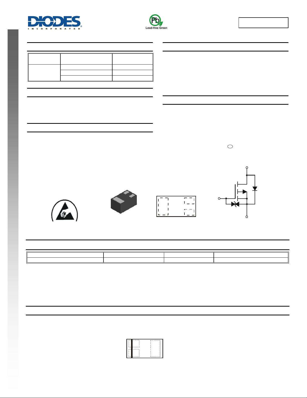
X1-DFN1006-3
Bottom View
Max
I
D
= +25C
-400mA
-300mA
-50mA
DMP32D4SFB
30V P-CHANNEL ENHANCEMENT MODE MOSFET
Features
Low On-Resistance
Ultra-Small Surfaced Mount Package
ESD Protected Gate
Totally Lead-Free & Fully RoHS Compliant (Notes 1 & 2)
Halogen and Antimony Free. “Green” Device (Note 3)
Qualified to AEC-Q101 Standards for High Reliability
Mechanical Data
Case: X1-DFN1006-3
Case Material: Molded Plastic, “Green” Molding Compound.
UL Flammability Classification Rating 94V-0
Moisture Sensitivity: Level 1 per J-STD-020
Terminal Connections: See Diagram
Terminals: Finish – NiPdAu over Copper leadframe. Solderable
per MIL-STD-202, Method 208
Weight: 0.001 grams (approximate)
S
D
G
Top View
e4
Gate
Gate
Protection
Diode
Equivalent Circuit
Drain
Source
Ordering Information (Note 4)
Product Marking Reel size (inches) Quantity per reel
DMP32D4SFB-7B XP 7 10,000
Notes: 1. No purposely added lead. Fully EU Directive 2002/95/EC (RoHS) & 2011/65/EU (RoHS 2) compliant.
2. See http://www.diodes.com/quality/lead_free.html for more information about Diodes Incorporated’s definitions of Halogen- and Antimony-free, "Green"
and Lead-free.
3. Halogen- and Antimony-free "Green” products are defined as those which contain <900ppm bromine, <900ppm chlorine (<1500ppm total Br + Cl) and
<1000ppm antimony compounds.
4. For packaging details, go to our website at http”//www.diodes.com/products/packages.html.
Marking Information
XP
Bar Denotes Gate and Source Side
DMP32D4SFB
Document number: DS36161 Rev. 2 - 2
Top View
1 of 6
www.diodes.com
XP = Product Type Marking Code
March 2013
© Diodes Incorporated

)
g
g
g
g
)
r
)
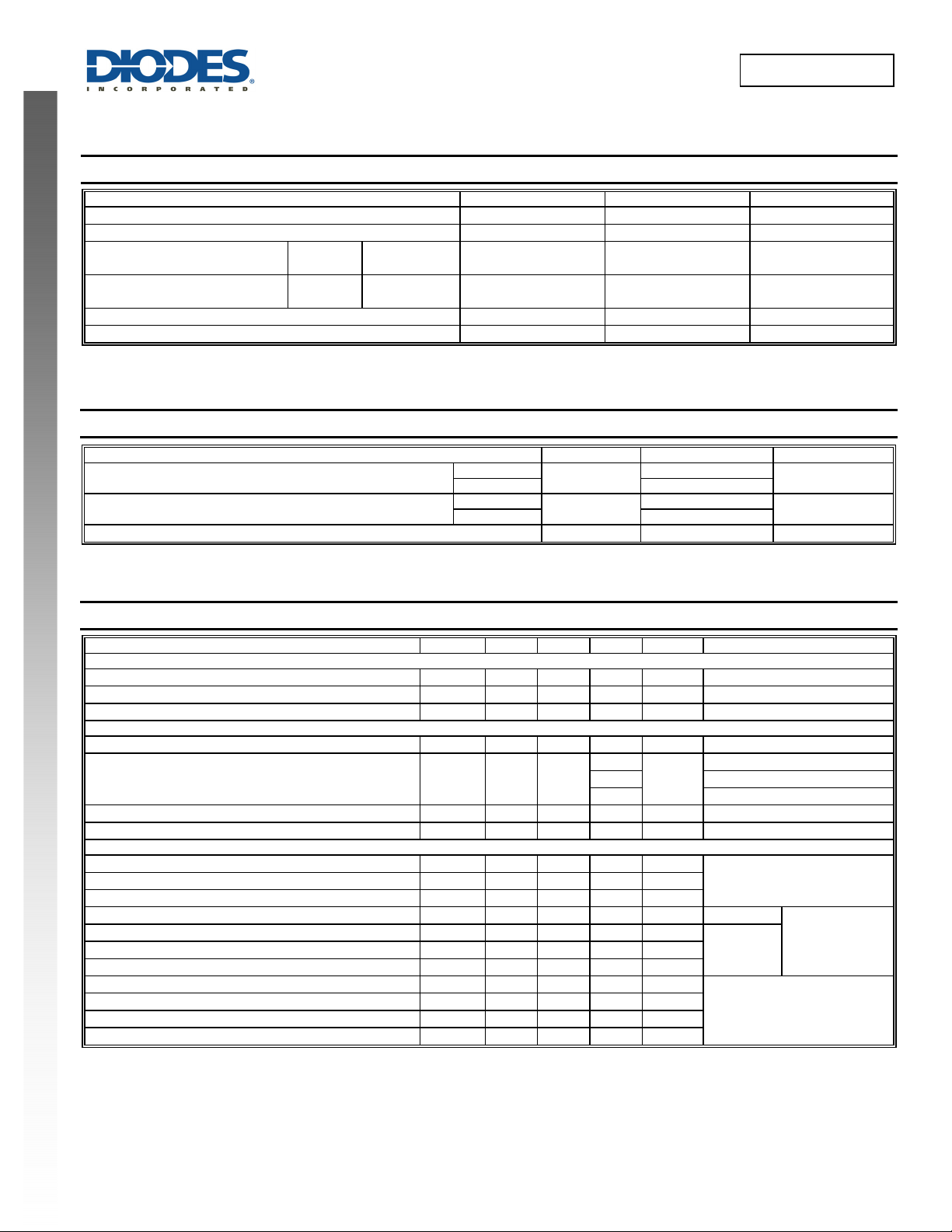
Maximum Ratings (@T
Characteristic Symbol Value Unit
Drain-Source Voltage
Gate-Source Voltage
Continuous Drain Current (Note 5)
Continuous Drain Current (Note 6)
Pulsed Drain Current (Note 5)
Maximum Body Diode continuous Current
Thermal Characteristics (@T
Total Power Dissipation
Thermal Resistance, Junction to Ambient
ADVANCE INFORMATION NEW PRODUCT
Operating and Storage Temperature Range
DMP32D4SFB
= +25°C, unless otherwise specified.)
A
V
DSS
V
GSS
= +25°C
T
V
= -10V
GS
V
= -10V
GS
= +25°C, unless otherwise specified.)
A
A
T
= +70°C
A
= +25°C
T
A
= +70°C
T
A
I
I
D
I
D
DM
I
S
Characteristic Symbol Value Units
(Note 5)
(Note 6) 1.2
(Note 5)
(Note 6) 105
P
R
T
J, TSTG
D
JA
-30 V
±20 V
-400
-300
-500
-400
mA
mA
-1 A
-800 mA
0.5
273
W
°C/W
-55 to 150 °C
Electrical Characteristics (@T
= +25°C, unless otherwise specified.)
A
Characteristic Symbol Min Typ Max Unit Test Condition
OFF CHARACTERISTICS (Note 7)
Drain-Source Breakdown Voltage
Zero Gate Voltage Drain Current TJ = +25°C I
Gate-Source Leakage
BV
I
DSS
DSS
GSS
-30 - - V
- - -1 µA
- - ±10 µA
VGS = 0V, ID = -1mA
VDS = -30V, VGS = 0V
VGS = ±16V, VDS = 0V
ON CHARACTERISTICS (Note 7)
Gate Threshold Voltage
Static Drain-Source On-Resistance
Forward Transfer Admittance
Diode Forward Voltage
V
GS(th
R
DS (ON)
|Y
V
fs
SD
-1.3 - -2.3 V
2.4
- -
4
16
|
- 6 - S
- 0.8 1.2 V
VDS = VGS, ID = -250μA
= -10V, ID = -200mA
V
Ω
GS
V
= -4.5V, ID = -200mA
GS
V
= -2.5V, ID = -10mA
GS
VDS = -10V, ID = -400mA
VGS = 0V, IS = -300mA
DYNAMIC CHARACTERISTICS (Note 8)
Input Capacitance
Output Capacitance
Reverse Transfer Capacitance
Total Gate Charge
Total Gate Charge
Gate-Source Charge
Gate-Drain Charge
Turn-On Delay Time
Turn-On Rise Time
Turn-Off Delay Time
Turn-Off Fall Time
Notes: 5. Device mounted on FR-4 PC board, with minimum recommended pad layout, single sided.
6. Device mounted on FR-4 substrate PC board, 2oz copper, with 1inch square copper pad layout
7 .Short duration pulse test used to minimize self-heating effect.
8. Guaranteed by design. Not subject to production testing.
C
C
C
Q
Q
Q
Q
t
D(on
t
D(off
iss
oss
rss
t
t
s
d
f
- 51 -
- 11 -
- 9 -
- 0.6 -
- 1.3 -
- 0.2 -
- 0.2 -
- 3.6 -
- 8.5 -
- 31.3 -
- 20.2 -
pF
pF
pF
nC
nC
nC
nC
ns
ns
ns
ns
= -15V, VGS = 0V,
V
DS
f = 1.0MHz
VGS = -4.5V
= -10V
V
GS
= -15V, I
V
DS
V
= -10V, RG = 1Ω
GS
D
V
= -10V,
DS
I
= -200mA
D
= -500mA
DMP32D4SFB
Document number: DS36161 Rev. 2 - 2
2 of 6
www.diodes.com
March 2013
© Diodes Incorporated
 Loading...