

Diodes DMP3099L User Manual

Product Summary
I
D
TA = +25°C
-3.8A
-3.0A
V
(BR)DSS
-30V
R
65m @ V
99m @ VGS = -4.5V
DS(ON)
max
= -10V
GS
Description
This MOSFET has been designed to minimize the on-state resistance
(R
) and yet maintain superior switching performance, making it
DS(ON)
ideal for high efficiency power management applications.
Applications
Backlighting
Power Management Functions
DC-DC Converters
NEW PRODUCT
SOT23
Top View
max
Equivalent Circuit
DMP3099L
P-CHANNEL ENHANCEMENT MODE MOSFET
Features and Benefits
Low Gate Threshold Voltage
Low Input Capacitance
Fast Switching Speed
Low Input/Output Leakage
Totally Lead-Free & Fully RoHS compliant (Notes 1 & 2)
Halogen and Antimony Free. “Green” Device (Note 3)
Qualified to AEC-Q101 Standards for High Reliability
Mechanical Data
Case: SOT23
Case Material: Molded Plastic, “Green” Molding Compound. UL
Flammability Classification Rating 94V-0
Moisture Sensitivity: Level 1 per J-STD-020
Terminals: Finish Matte Tin annealed over Copper leadframe.
Solderable per MIL-STD-202, Method 208
Terminal Connections: See Diagram
Weight: 0.008 grams (approximate)
D
G
Top View
Pin Configuration
S
e3
Ordering Information (Note 4)
Part Number Compliance Case Packaging
DMP3099L-7 Standard SOT23 3000/Tape & Reel
DMP3099L-13 Standard SOT23 10000/Tape & Reel
Notes: 1. No purposely added lead. Fully EU Directive 2002/95/EC (RoHS) & 2011/65/EU (RoHS 2) compliant.
2. See http://www.diodes.com/quality/lead_free.html for more information about Diodes Incorporated’s definitions of Halogen- and Antimony-free, "Green"
and Lead-free.
3. Halogen- and Antimony-free "Green” products are defined as those which contain <900ppm bromine, <900ppm chlorine (<1500ppm total Br + Cl) and
<1000ppm antimony compounds.
4. For packaging details, go to our website at http”//www.diodes.com/products/packages.html.
Marking Information
Date Code Key
Year 2008 2009 2010 2011 2012 2013 2014 2015
Code V W X Y Z A B C
Month Jan Feb Mar Apr May Jun Jul Aug Sep Oct Nov Dec
Code 1 2 3 4 5 6 7 8 9 O N D
DMP3099L
Document number: DS36081 Rev. 3 - 2
D99
D99= Product Type Marking Code
YM = Date Code Marking
YM
Y = Year (ex: V = 2008)
M = Month (ex: 9 = September)
1 of 6
www.diodes.com
May 2013
© Diodes Incorporated
)
g
g
)
)
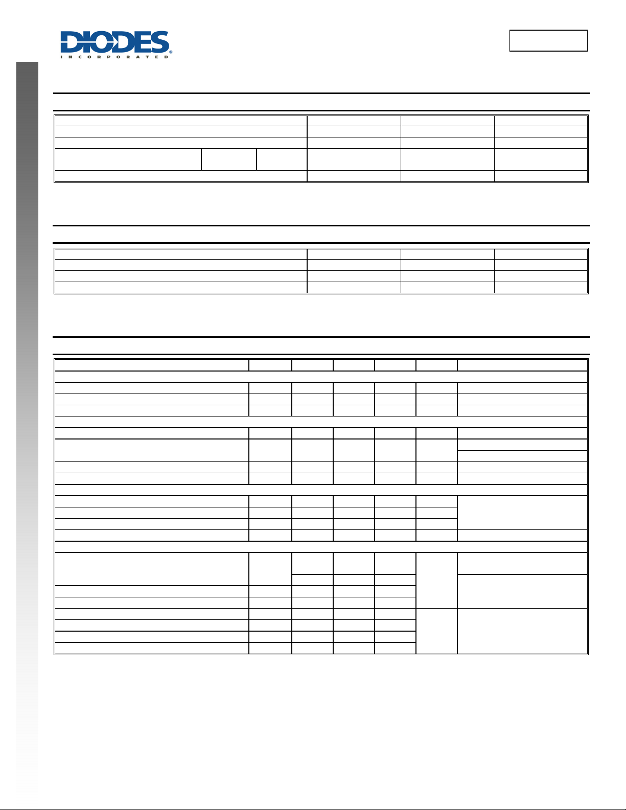
Maximum Ratings (@T
Drain-Source Voltage
Gate-Source Voltage
Drain Current (Note 5) VGS = -10V
Pulsed Drain Current (Note 6)
= +25°C, unless otherwise specified.)
A
Characteristic Symbol Value Units
T
Steady
State
= +25°C
A
= +70°C
T
A
Thermal Characteristics
Characteristic Symbol Value Units
Total Power Dissipation (Note 5)
Thermal Resistance, Junction to Ambient @TA = +25°C (Note 5) R
Operating and Storage Temperature Range
NEW PRODUCT
V
V
I
P
T
J, TSTG
DSS
GSS
I
D
DM
D
JA
DMP3099L
-30 V
±20 V
-3.8
-2.9
-11 A
1.08 W
115 °C/W
-55 to +150 °C
A
Electrical Characteristics (@T
= +25°C, unless otherwise specified.)
A
Characteristic Symbol Min Typ Max Unit Test Condition
OFF CHARACTERISTICS (Note 7)
Drain-Source Breakdown Voltage BV
Zero Gate Voltage Drain Current I
Gate-Source Leakage I
-30 — — V V
DSS
— — -800 nA VDS = -30V, VGS = 0V
DSS
— — ±100 nA VGS = ±20V, VDS = 0V
GSS
= 0V, ID = -250µA
GS
ON CHARACTERISTICS (Note 7)
Gate Threshold Voltage V
Static Drain-Source On-Resistance R
-1.0 — -2.1 V V
GS(th
— —
DS(ON)
65
99
m
= VGS, ID = -250µA
DS
= -10V, ID = -3.8A
V
GS
V
= -4.5V, ID = -3.0A
GS
Forward Transfer Admittance |Yfs| — 3.6 — S VDS = -5V, ID = -2.7A
Diode Forward Voltage (Note 6) VSD — — -1.26 V V
= 0V, IS = -2.7A
GS
DYNAMIC CHARACTERISTICS (Note 8)
Input Capacitance C
Output Capacitance C
Reverse Transfer Capacitance C
— 563 — pF
iss
— 48 — pF
oss
— 41 — pF
rss
VDS = -25V, VGS = 0V,
f = 1.0MHz
Gate Resistance RG —10.3 — VGS = 0V VDS = 0V, f = 1MHz
SWITCHING CHARACTERISTICS (Note 8)
V
= -15V, VGS = -4.5V,
Total Gate Charge Qg
— 5.2 —
— 11 —
Gate-Source Charge Q
Gate-Drain Charge Q
Turn-On Delay Time t
— 1.7 —
s
— 1.9 —
d
— 4.8 —
d(on
Rise Time tr —5.0 —
Turn-Off Delay Time t
— 31 —
d(off
nC
ns
DS
I
= -3.8A
D
V
= -15V, VGS = -10V,
DS
I
= -3.8A
D
= -15V, VGS = -10V,
V
DS
= -1A, RG = 6.0
I
D
Fall Time tf —15 —
Notes: 5. Device mounted on FR-4 PCB on 2 oz., 0.5 in.2 copper pads and t ≤5 sec.
6. Pulse width ≤10µS, Duty Cycle ≤1%.
7. Short duration pulse test used to minimize self-heating effect.
8. Guaranteed by design. Not subject to production testing.
DMP3099L
Document number: DS36081 Rev. 3 - 2
2 of 6
www.diodes.com
May 2013
© Diodes Incorporated
 Loading...