

Page 1
P-CHANNEL ENHANCEMENT MODE MOSFET
Features
• Low R
• 65mΩ @V
• 115mΩ @V
• Low Input/Output Leakage
• Lead Free By Design/RoHS Compliant (Note 3)
• Qualified to AEC-Q101 Standards for High Reliability
• "Green" Device (Note 4)
DS(ON)
:
= -10V
GS
= -4.5V
GS
UCT NEW PROD
Maximum Ratings @T
= 25°C unless otherwise specified
A
Characteristic Symbol Value Unit
Drain-Source Voltage
Gate-Source Voltage
Drain Current (Note 1) Continuous TA = 25°C
T
Pulsed Drain Current (Note 2)
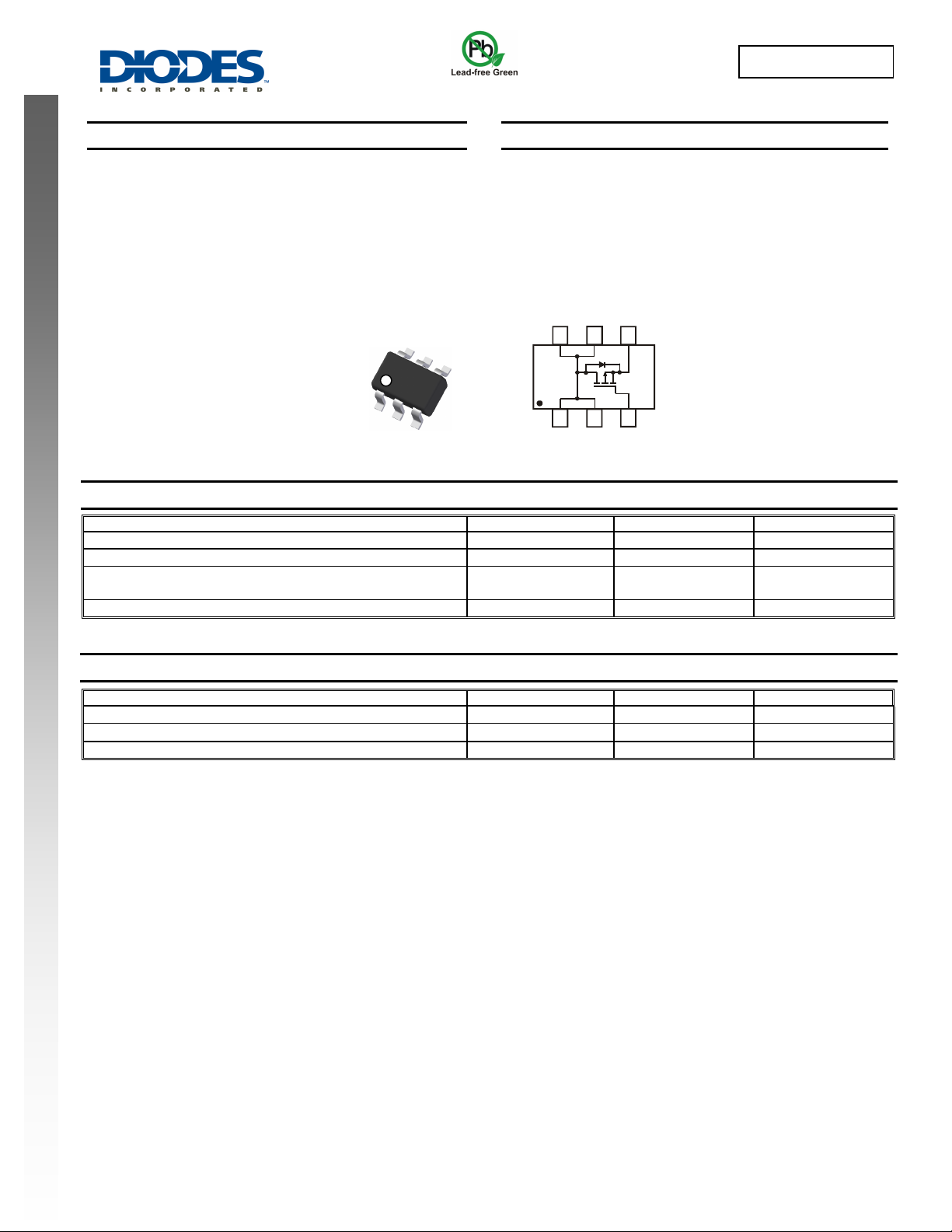
TOP VIEW
= 70°C
A
Mechanical Data
• Case: SOT-26
• Case Material - Molded Plastic. UL Flammability Rating 94V-0
• Moisture Sensitivity: Level 1 per J-STD-020D
• Terminals: Finish - Matte Tin Solderable per MIL-STD-202,
Method 208
• Terminal Connections: See Diagram
• Marking Information: See Page 4
• Ordering Information: See page 4
• Weight: 0.008 grams (approximate)
SOT-26
V
DSS
V
GSS
I
D
I
DM
D
D
D
D
TOP VIEW
Internal Schematic
DMP3098LDM
S
G
-30 V
±20
-4.0
-3.0
-14 A
V
A
Thermal Characteristics
Characteristic Symbol Value Unit
Total Power Dissipation (Note 1)
Thermal Resistance, Junction to Ambient (Note 1); Steady-State
Operating and Storage Temperature Range
Notes: 1. Device mounted on 1"x1", FR-4 PC board on 0.1in.2 pads on 2 oz. Copper pads and test pulse width t ≤10s.
2. Repetitive Rating, pulse width limited by junction temperature.
3. No purposefully added lead.
4. Diodes Inc's "Green" policy can be found on our website at http://www.diodes.com/products/lead_free/index.php.
P
D
R
JA
θ
, T
T
J
STG
1.25 W
100
-55 to +150
DMP3098LDM
Document number: DS31446 Rev. 3 - 2
1 of 4
www.diodes.com
°C/W
°C
October 2008
© Diodes Incorporated
Page 2
RAIN CUR
REN
T
Electrical Characteristics @T
STATIC PARAMETERS
Drain-Source Breakdown Voltage
Gate-Body Leakage Current
Gate Threshold Voltage
On State Drain Current (Note 5)
Static Drain-Source On-Resistance (Note 5)
Forward Transconductance (Note 5)
Diode Forward Voltage (Note 5)
DYNAMIC PARAMETERS (Note 6)
Input Capacitance
Output Capacitance
Reverse Transfer Capacitance
NEW PRODUCT
Gate Resistance
SWITCHING CHARACTERISTICS
Total Gate Charge
Gate-Source Charge
Gate-Drain Charge
Turn-On Delay Time
Rise Time
Turn-Off Delay Time
Fall Time
Notes: 5. Test pulse width t = 300μs.
6. Guaranteed by design. Not subject to production testing.
20
16
12
Characteristic Symbol Min Typ Max Unit Test Condition
V = -10V
GS
= 25°C unless otherwise specified
A
-30
BV
DSS
g
⎯ ⎯
⎯ ⎯
-1.0
-15
⎯
⎯
⎯
⎯
⎯
⎯
⎯
⎯
⎯
⎯
⎯
⎯
⎯
⎯
V = -4.5V
GS
I
I
V
GS(th)
I
D (ON)
R
DS (ON)
g
V
C
C
C
Q
Q
t
d(on)
t
d(off)
DSS
GSS
FS
SD
iss
oss
rss
R
Q
gd
t
t
G
gs
r
f
⎯ ⎯
±100
⎯
-2.1 V
⎯ ⎯
56
98
115
5.3
-1
65
⎯
V
μA
nA
A
mΩ
S
0.79 -1.2 V
336
70
49
4.6
4.0
7.8
1.0
2.5
6.0
5.0
17.6
9.5
⎯
⎯
⎯
⎯ Ω
⎯
⎯
⎯
⎯
⎯
⎯
⎯
pF
pF
pF
nC
ns
20
V = -5V
DS
16
(A)
12
DMP3098LDM
ID = -250μA, VGS = 0V
V
= -30V, VGS = 0V Zero Gate Voltage Drain Current TJ = 25°C
DS
V
= 0V, VGS = ±20V
DS
V
= VGS, ID = -250μA
DS
V
= -4.5V, VDS = -5V
GS
V
= -10V, ID = -4.0A
GS
V
= -4.5V, ID = -3.0A
GS
V
= -10V, ID = -4.0A
DS
IS = -1.7A, V
V
= -25V, VGS = 0V
DS
f = 1.0MHz
VDS = 0V, VGS = 0V, f = 1.0MHz
V
= -15V, VGS = -4.5V, ID = -5.0A
DS
= -15V, VGS = -10V, ID = -5.0A
V
DS
VDS = -15V, VGS = -4.5V, ID = -5.0A
VDS = -15V, VGS = -4.5V, ID = -5.0A
V
= -15V, VGS = -10V,
DS
I
= -1.0A, RG = 6.0Ω
D
T = 125°C
GS
T = 150°C
A
A
= 0V
T = -55°C
A
T = 25°C
A
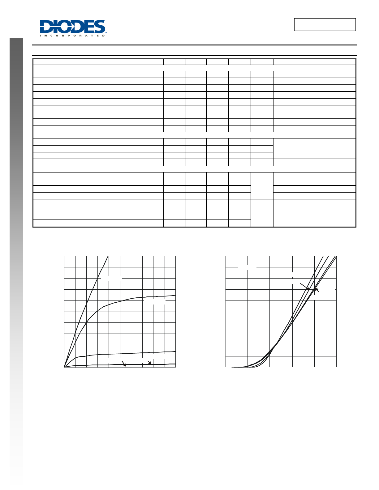
8
D
-I , DRAIN CURRENT (A)
4
V = -3.0V
V = -1.5V
GS
V = -2.5V
GS
GS
0
01 2 3 4
-V , DRAIN-SOURCE VOLTAGE (V)
DS
Fig. 1 Typical Output Characteristics
5
8
D
-I , D
4
0
12 3 456
-V , GATE SOURCE VOLTAGE (V)
GS
Fig. 2 Typical Transfer Characteristics
DMP3098LDM
Document number: DS31446 Rev. 3 - 2
2 of 4
www.diodes.com
October 2008
© Diodes Incorporated
Page 3

R
TATIC DR
OUR
C
R
TATIC DR
O
URC
C, CAPACITAN
C
F
GAT
T
H
RESH
O
OLT
G
O
U
R
CE C
URR
T
NEW PRODUCT
DMP3098LDM
1
E
Ω
V = -4.5V
GS
AIN-S
0.14
T = 150°C
A
0.12
E
0.10
Ω
AIN-S
0.08
T = 125°C
A
T = 85°C
A
T = 25°C
A
0.1
, S
0.06
V = -10V
ON-RESISTANCE ( )
DS(ON)
GS
, S
ON-RESISTANCE ( )
0.04
DS(ON)
T = -55°C
A
0.02
0.01
04 81216
-I , DRAIN CURRENT (A)
D
Fig. 3 Typical On-Resistance
vs. Drain Current and Gate Voltage
1.6
20
0
0246810
-I , DRAIN CURRENT (A)
D
Fig. 4 Typical On-Resi stance
vs. Drain Current and Temperature
1,000
1.4
V = -10V
GS
I = -5.3A
D
1.2
1.0
DS(ON)
0.8
R , STATIC DRAIN-SOURCE
ON-RESISTANCE (NORMALIZED)
0.6
-50 -25 0 25 50 75 100 125 150
T , AMBIENT TEMPERATURE (°C)
A
Fig. 5 On-Resistance Variation with Temperature
2.4
E (V)
A
2.0
I = -250µA
D
LD V
1.6
V = -4.5V
GS
I = -4.2A
D
C
)
iss
E (p
100
C
oss
C
rss
10
0 5 10 15 20 25 30
-V , DRAIN-SOURCE VOLTAGE (V)
DS
Fig. 6 Typical Capacitance
10
8
(A)
EN
6
T = 25°C
A
4
E
1.2
GS(TH)
-V ,
0.8
-50 -25 0 25 50 75 100 125 150
T , AMBIENT TEMPERATURE (°C)
Fig. 7 Gate Threshold Variation vs. Ambient Temperature
A
S
-I , S
2
0
0.4 0.6 0.8 1 1.2
-V , SOURCE-DRAIN VOLTAGE (V)
SD
Fig. 8 Diode Forward Voltage vs. Current
DMP3098LDM
Document number: DS31446 Rev. 3 - 2
3 of 4
www.diodes.com
October 2008
© Diodes Incorporated
Page 4

DMP3098LDM
Ordering Information (Note 7)
Part Number Case Packaging
DMP3098LDM-7 SOT-26 3000/Tape & Reel
Notes: 7. For packaging details, go to our website at http://www.diodes.com/datasheets/ap02007.pdf.
Marking Information
NEW PRODUCT
Date Code Key
Year 2008 2009 2010 2011 2012 2013 2014 2015
Code V W X Y Z A B C
Month Jan Feb Mar Apr May Jun Jul Aug Sep Oct Nov Dec
Code 1 2 3 4 5 6 7 8 9 O N D
DMB
DMB = Product Type Marking Code
YM = Date Code Marking
YM
Y = Year (ex: V = 2008)
M = Month (ex: 9 = September)
Package Outline Dimensions
K
J
A
SOT-26
B C
H
M
D
L
Dim Min Max Typ
A 0.35 0.50 0.38
B 1.50 1.70 1.60
C 2.70 3.00 2.80
D
⎯ ⎯
H 2.90 3.10 3.00
J 0.013 0.10 0.05
K 1.00 1.30 1.10
L 0.35 0.55 0.40
M 0.10 0.20 0.15
0° 8°
α
All Dimensions in mm
0.95
⎯
Suggested Pad Layout
Diodes Incorporated and its subsidiaries reserve the right to make modifications, enhancements, improvements, corrections or other changes
without further notice to any product herein. Diodes Incorporated does not assume any liability arising out of the application or use of any product
described herein; neither does it convey any license under its patent rights, nor the rights of others. The user of products in such applications shall
assume all risks of such use and will agree to hold Diodes Incorporated and all the companies whose products are represented on our website,
harmless against all damages.
Diodes Incorporated products are not authorized for use as critical components in life support devices or systems without the expressed written
approval of the President of Diodes Incorporated.
G
Z
Y
X
EE
Dimensions Value (in mm)
C
IMPORTANT NOTICE
LIFE SUPPORT
Z
G
X
Y
C 2.40
E
3.20
1.60
0.55
0.80
0.95
DMP3098LDM
Document number: DS31446 Rev. 3 - 2
4 of 4
www.diodes.com
October 2008
© Diodes Incorporated
 Loading...