Diodes DMP3010LPS User Manual

Product Summary
I
V
R
(BR)DSS
-30V
7.5m @ V
10m @ VGS = -4.5V
DS(ON)
GS
= -10V
D
TA = +25°C
-36A
-31A
Description
This new generation 30V P-Channel Enhancement Mode MOSFET
has been designed to minimize R
switching performance. This device is ideal for use in notebook
battery power management and loadswitch.
and yet maintain superior
DS(ON)
Applications
• Notebook Battery Power Management
• DC-DC Converters
• Loadswitch
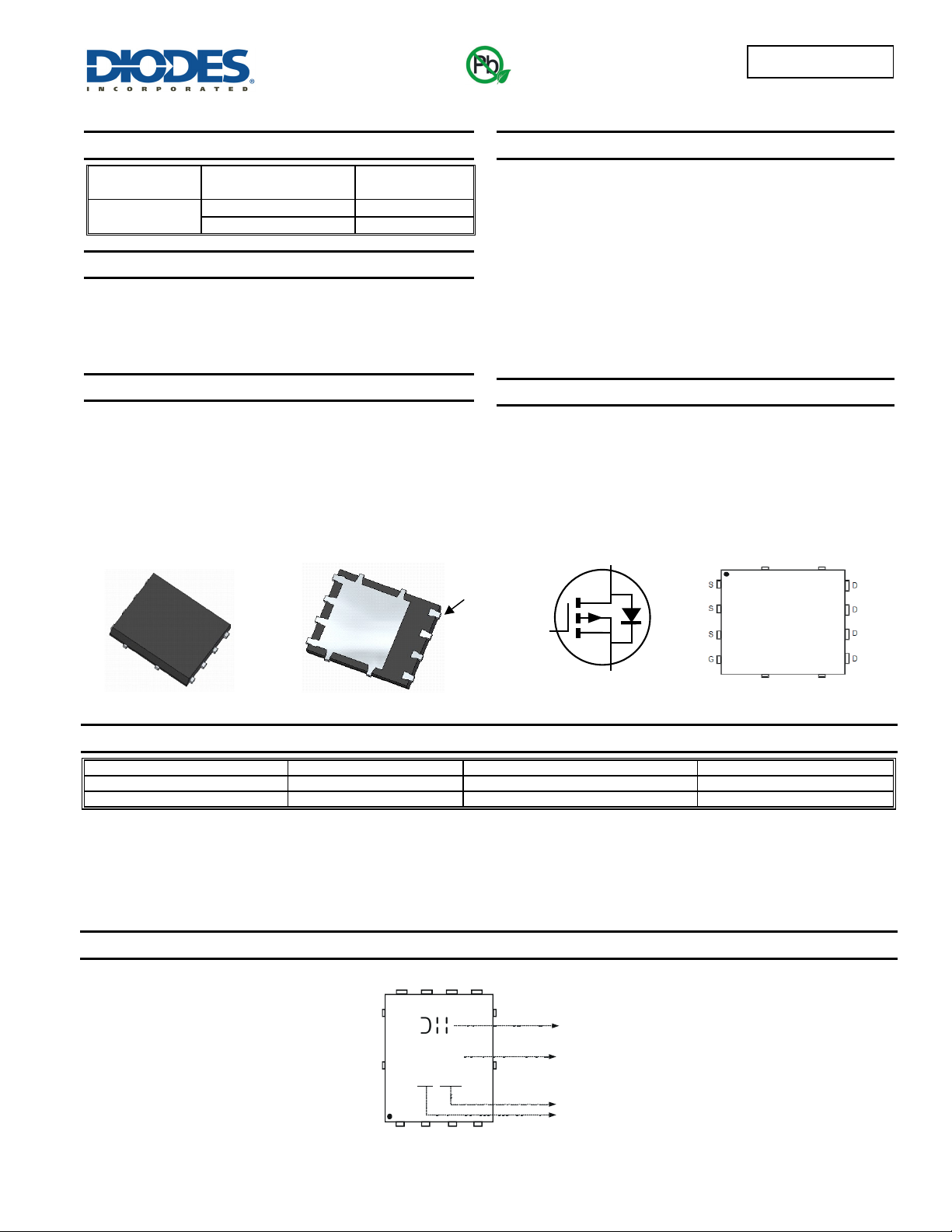
Top View
POWERDI5060-8
Pin1
Bottom View
Ordering Information (Note 4 & 5)
DMP3010LPS
Green
Features
• Thermally Efficient Package-Cooler Running Applications
• High Conversion Efficiency
• Low
• Low Input Capacitance
• Fast Switching Speed
• <1.1mm Package Profile – Ideal for Thin Applications
• ESD HBM Protected up to 1kV
• Lead-Free Finish; RoHS Compliant (Notes 1 & 2)
• Halogen and Antimony Free. “Green” Device (Note 3)
• Qualified to AEC-Q101 Standards for High Reliability
P-CHANNEL ENHANCEMENT MODE MOSFET
– Minimizes On State Losses
RDS(ON)
Mechanical Data
• Case: POWERDI5060-8
• Case Material: Molded Plastic, “Green” Molding Compound. UL
Flammability Classification Rating 94V-0
• Moisture Sensitivity: Level 1 per J-STD-020
• Terminal Connections: See Diagram Below
• Weight: 0.097 grams (approximate)
D
G
S
Internal Schematic
Top View
Pin Configuration
POWERDI
®
Part Number Qualification Case Packaging
DMP3010LPS-13 Commercial POWERDI5060-8 2500 / Tape & Reel
DMP3010LPSQ-13 Automotive POWERDI5060-8 2500 / Tape & Reel
Notes: 1. EU Directive 2002/95/EC (RoHS) & 2011/65/EU (RoHS 2) compliant. All applicable RoHS exemptions applied.
2. See http://www.diodes.com/quality/lead_free.html for more information about Diodes Incorporated’s definitions of Halogen- and Antimony-free, "Green"
and Lead-free.
3. Halogen- and Antimony-free "Green” products are defined as those which contain <900ppm bromine, <900ppm chlorine (<1500ppm total Br + Cl) and
<1000ppm antimony compounds.
5. Automotive products are AEC-Q101 qualified and are PPAP capable. Automotive, AEC-Q101 and standard products are electrically and thermally
4. For packaging details, go to our website at http://www.diodes.com/products/packages.html.
the same, except where specified. For more information, please refer to http://www.diodes.com/quality/product_compliance_definitions/
Marking Information
POWERDI is a registered trademark of Diodes Incorporated.
DMP3010LPS
Document number: DS32239 Rev. 10 - 2
DDD
P4015SP
P3010LS
YY
WW
SDSSG
1 of 7
www.diodes.com
Logo
Part no.
Xth week: 01 ~ 53
Year: “09” = 2009
Year: “13” = 2013
November 2013
© Diodes Incorporated

)
g
g
g
)
r
)
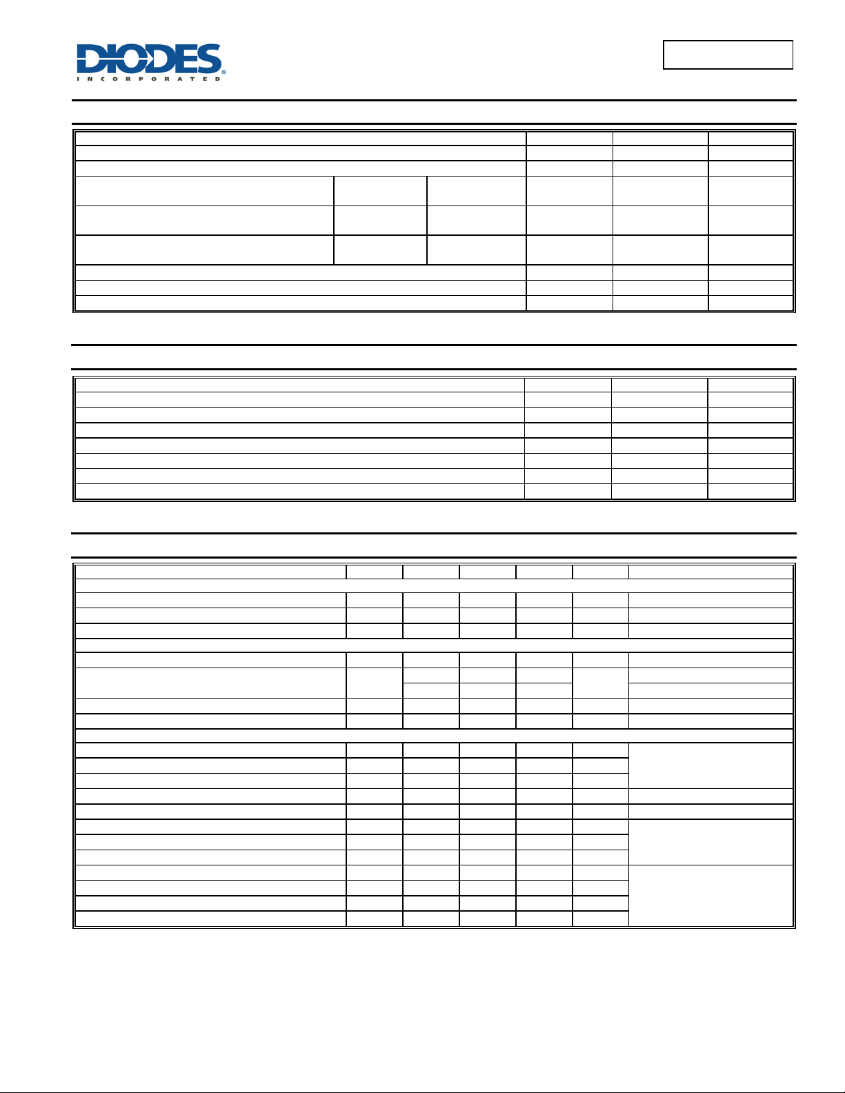
Maximum Ratings (@T
= +25°C, unless otherwise specified.)
A
Characteristic Symbol Value Unit
Drain-Source Voltage
Gate-Source Voltage
= +25°C
Continuous Drain Current (Note 7) VGS = 10V
Continuous Drain Current (Note 7) VGS = 4.5V
Continuous Drain Current (Note 6) VGS = 10V
Steady
State
Steady
State
Steady
State
T
A
T
= +70°C
A
T
= +25°C
A
= +70°C
T
A
= +25°C
T
A
T
= +70°C
A
Pulsed Drain Current (Notes 6 & 9)
Avalanche Current (Notes 10 & 11)
Repetitive Avalanche Energy (Notes 10 & 11) L = 1mH
Thermal Characteristics
Characteristic Symbol Value Unit
Power Dissipation (Note 6)
Thermal Resistance, Junction to Ambient @TA = +25°C (Note 6) R
Power Dissipation (Note 7)
Thermal Resistance, Junction to Ambient @TA = +25°C (Note 7) R
Power Dissipation (Notes 7 & 8)
Thermal Resistance, Junction to Case @TC = +25°C (Notes 7 & 8) R
Operating and Storage Temperature Range
T
DMP3010LPS
V
DSS
V
GSS
I
D
I
D
I
D
I
DM
I
AR
E
AR
P
D
JA
P
D
JA
P
D
JC
, T
J
STG
-30 V
±20 V
-36
-29
-31
-25
-14.5
-11.5
A
A
A
-100 A
-17.5 A
153 mJ
2.18 W
55 °C/W
14.37 W
8.7 °C/W
58.7 W
2.13 °C/W
-55 to +150 °C
Electrical Characteristics (@T
= +25°C, unless otherwise specified.)
A
Characteristic Symbol Min Typ Max Unit Test Condition
OFF CHARACTERISTICS (Note 11)
Drain-Source Breakdown Voltage
Zero Gate Voltage Drain Current
Gate-Source Leakage
BV
I
I
GSS
DSS
DSS
-30 — — V
— —
— —
-1.0 A
±100 nA
VGS = 0V, ID = -250µA
VDS = -30V, VGS = 0V
VGS = ±20V, VDS = 0V
ON CHARACTERISTICS (Note 11)
Gate Threshold Voltage
Static Drain-Source On-Resistance
Forward Transfer Admittance
Diode Forward Voltage
V
GS(th
R
DS(ON)
|Y
V
fs
SD
-1.1 -1.6 -2.1 V
—
—
|
—
—
5.7 7.5
7.2 10
30 — S
-0.65 -1.0 V
VDS = VGS, ID = -250µA
V
= -10V, ID = -10A
m
GS
V
= -4.5V, ID = -10A
GS
VDS = -15V, ID = -10A
VGS = 0V, IS = -1A
DYNAMIC CHARACTERISTICS (Note 12)
Input Capacitance
Output Capacitance
Reverse Transfer Capacitance
Gate Resistance
C
iss
C
oss
C
rss
R
Total Gate Charge (VGS = -10V) Qg
Total Gate Charge (VGS = -4.5V) Qg
Gate-Source Charge
Gate-Drain Charge
Turn-On Delay Time
Turn-On Rise Time
Turn-Off Delay Time
Turn-Off Fall Time
Notes: 6. Device mounted on FR-4 PCB with 1 inch square 2 oz. Copper, single sided.
7. Device mounted on FR-4 PCB with infinite heatsink.
8. R
9. Repetitive rating, pulse width limited by junction temperature, 10μs pulse, duty cycle = 1%.
10. I
11. Short duration pulse test used to minimize self-heating effect.
is guaranteed by design while R
JC
and EAR rating are based on low frequency and duty cycles to keep TJ = +25°C.
AR
12. Guaranteed by design. Not subject to production testing.
is determined by the user’s board design.
CA
Q
Q
t
D(on
t
D(off
s
d
t
t
f
—
—
—
—
—
—
—
—
—
—
—
—
6234
1500
774
1.28
126.2
59.2
16.1
15.7
11.4
9.4
260.7
99.3
—
—
—
—
—
—
—
—
—
—
—
—
pF
V
= 15V, VGS = 0V,
pF
pF
nC
nC
nC
nC
DS
f = 1.0MHz
VDS = 0V, VGS = 0V, f = 1MHz
VDS = -15V, ID = -10A
= -15V, VGS = -4.5V,
V
DS
I
= -10A
D
ns
ns
ns
= -15V, V
V
DS
= 6, ID = -1A
R
G
ns
GEN
= -10V,
POWERDI is a registered trademark of Diodes Incorporated.
DMP3010LPS
Document number: DS32239 Rev. 10 - 2
2 of 7
www.diodes.com
November 2013
© Diodes Incorporated

D
RAIN CUR
REN
T
R
CUR
R
T
R
R
OUR
CE ON-R
TANC
R
R
OUR
CE ON-R
TANC
R
RAIN
OUR
C
DMP3010LPS
(A)
30
25
20
15
V = -10V
GS
V = -4.5V
GS
V = -5.0V
GS
V = -3.5V
GS
V = -3.0V
GS
V = -2.5V
GS
(A)
EN
30
25
20
15
V = -5V
DS
AIN
10
D
-I ,
5
V = -2.0V
0
0 0.5 1 1.5 2 2.5 3 3.5 4
-V , DRAIN-SOURCE VOLTAGE (V)
DS
GS
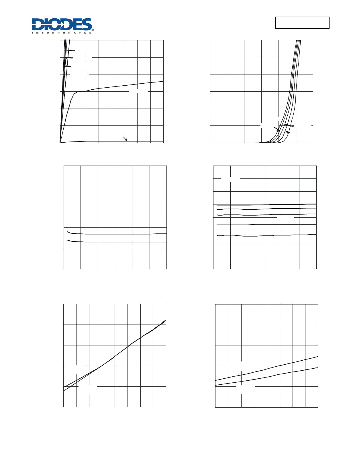
Fig. 1 Typical Output Characteristic
0.020
Ω
E ( )
10
D
-I , D
5
T = 150°C
A
T = 125°C
A
0
0 0.5 1 1.5 2 2.5 3
-V , GATE-SOURCE VOLTAGE (V)
GS
Fig. 2 Typical Transfer Characteristic
0.016
Ω
E ( )
0.014
V = -4.5V
GS
T = 85°C
A
T = 25°C
A
T = -55°C
A
0.016
0.012
ESIS
AIN-S
, D
DS(ON)
0.012
0.008
V = -4.5V
GS
V = -10V
0.004
0
0 5 10 15 20 25 30
-I , DRAIN-SOURCE CURRENT (A)
D
Fig. 3 Typical On-Resistance
GS
vs. Drain Current and Gate Voltage
ESIS
0.010
0.008
0.006
AIN-S
0.004
, D
0.002
DS(ON)
0
0 5 10 15 20 25 30
-I , DRAIN CURRENT (A)
D
T = 150°C
A
T = 125°C
A
T = 85°C
A
T = 25°C
A
T = -55°C
A
Fig. 4 Typical On-Resistance
vs. Drain Current and Temperature
1.6
1.4
0.020
0.016
E
1.2
1.0
V = -10V
GS
I = -20A
DSON
R , DRAIN-SOURCE
D
0.8
ON-RESISTANCE (NORMALIZED)
0.6
-50 -25 0 25 50 75 100 125 150
V = -4.5V
GS
I = -10A
D
T , AMBIENT TEMPERATURE (°C)
A
Fig. 5 On-Resistance Variation with Temperature
-S
, D
DSON
0.012
V = -4.5V
0.008
0.004
ON-RESISTANCE (NORMALIZED)
GS
I = -10A
D
V = -10V
GS
I = -20A
D
0
-50 -25 0 25 50 75 100 125 150
T , JUNCTION TEMPERATURE (°C)
J
Fig. 6 On-Resistance Variation with Temperature
POWERDI is a registered trademark of Diodes Incorporated.
DMP3010LPS
Document number: DS32239 Rev. 10 - 2
3 of 7
www.diodes.com
November 2013
© Diodes Incorporated
 Loading...