

Page 1
D
G
G
D
Product Summary
I
V
(BR)DSS
-30V
R
8mΩ @ V
10.2mΩ @ VGS = -4.5V
DS(on) max
GS = -10V -17A
D
TA = 25°C
-14.5A
Description and Applications
This new generation MOSFET has been designed to minimize the onstate resistance (R
performance, making it ideal for high efficiency power management
applications.
• DC-DC Converters
• Power management functions
• Backlighting
) and yet maintain superior switching
DS(on)
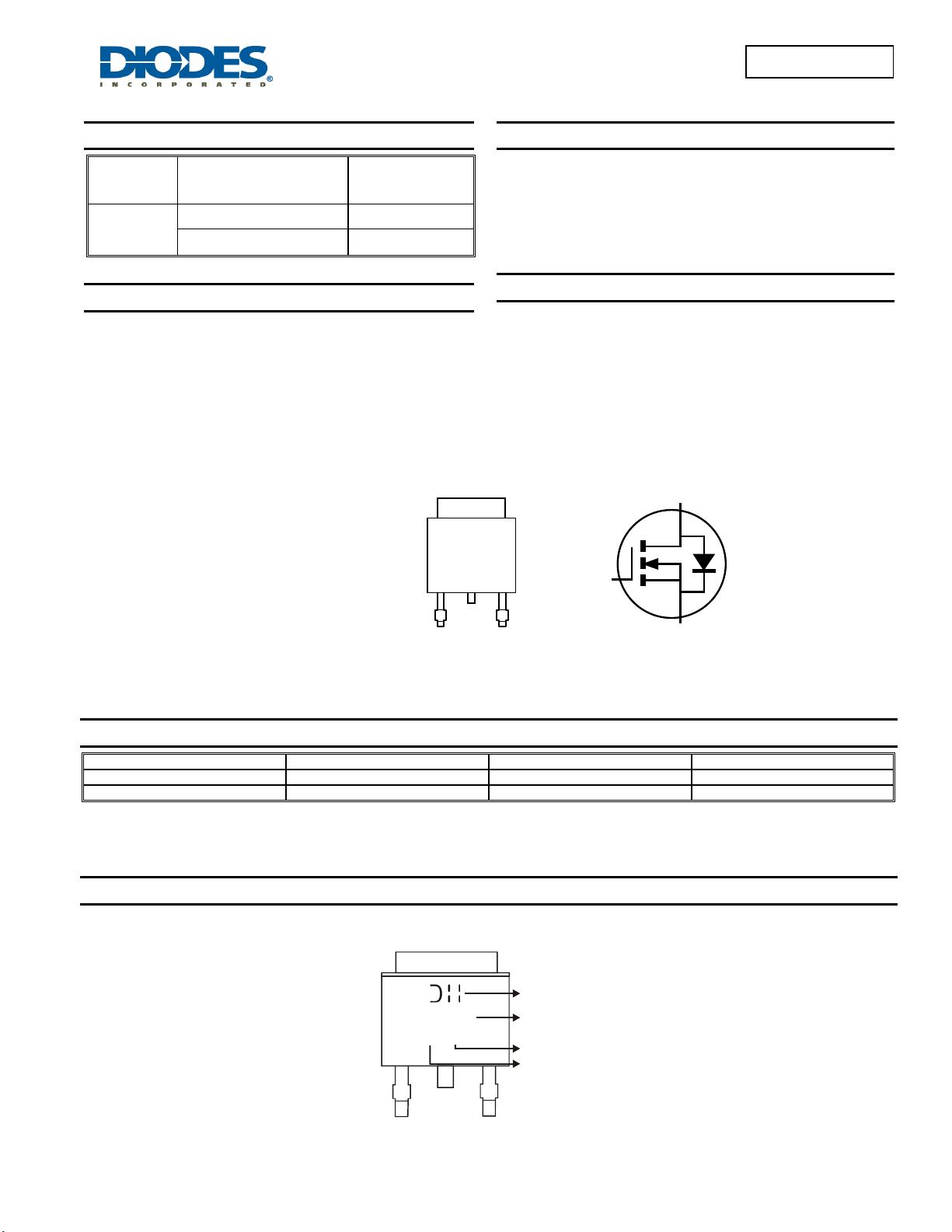
TO252
Top View
Top View
Pin-Out
DMP3010LK3
P-CHANNEL ENHANCEMENT MODE MOSFET
Features and Benefits
• Low Input Capacitance
• Low On-Resistance
• Fast Switching Speed
• "Green" Device (Note 1)
• Qualified to AEC-Q101 Standards for High Reliability
Mechanical Data
• Case: TO252 (DPAK)
• Case Material: Molded Plastic, “Green” Molding Compound. UL
Flammability Classification Rating 94V-0
• Moisture Sensitivity: Level 1 per J-STD-020
• Terminal Connections: See Diagram
• Terminals: Finish – Tin Finish annealed over Copper leadframe.
Solderable per MIL-STD-202, Method 208
• Weight: 0.33 grams (approximate)
D
S
Equivalent Circuit
S
Ordering Information (Note 2)
Part Number Qualification Case Packaging
DMP3010LK3-13 Commercial TO252 2,500/Tape & Reel
DMP3010LK3Q-13 Automotive TO252 2,500/Tape & Reel
Notes: 1. Diodes Inc.’s “Green” policy can be found on our website at http://www.diodes.com.
2. For packaging details, go to our website at http://www.diodes.com.
Marking Information
DMP3010LK3
Document number: DS35716 Rev. 4 - 2
P3010L
YYWW
1 of 7
www.diodes.com
Logo
Part no.
Xth week: 01 ~ 53
Year: “11” = 2011
.
February 2012
© Diodes Incorporated
Page 2
)
g
g
g
)
r
)
Maximum Ratings @T
= 25°C unless otherwise specified
A
Characteristic Symbol Value Units
Drain-Source Voltage
Gate-Source Voltage
Continuous Drain Current (Note 4) VGS = -10V
Continuous Drain Current (Note 4) VGS = -4.5V
Pulsed Drain Current (10μs pulse, duty cycle = 1%)
Maximum Body Diode Forward Current (Note 4)
Avalanche Current (Note 5)
Avalanche Energy (Note 5)
Thermal Characteristics @T
= 25°C unless otherwise specified
A
Characteristic Symbol Value Units
Total Power Dissipation (Note 3)
Thermal Resistance, Junction to Ambient (Note 3)
Total Power Dissipation (Note 4)
Thermal Resistance, Junction to Ambient (Note 4)
Operating and Storage Temperature Range
Steady
State
t<10s
Steady
State
t<10s
DMP3010LK3
V
DSS
V
GSS
T
= 25°C
A
= 70°C
T
A
= 25°C
T
A
T
= 70°C
A
T
= 25°C
A
= 70°C
T
A
= 25°C
T
A
T
= 70°C
A
Steady state
t<10s 29 °C/W
Steady state
t<10s 15 °C/W
E
I
I
I
I
I
I
DM
I
AS
D
D
D
D
S
AS
R
R
T
J, TSTG
P
D
JA
θ
P
D
JA
θ
-30 V
±20 V
-17.0
-13.0
-27.0
-21.0
-14.5
-11.5
-23.0
-18.0
A
A
A
A
-100 A
5.5 A
47 A
113 mJ
1.7 W
72 °C/W
3.4 W
37 °C/W
-55 to +150 °C
Electrical Characteristics @T
= 25°C unless otherwise specified
A
Characteristic Symbol Min Typ Max Unit Test Condition
OFF CHARACTERISTICS (Note 6)
Drain-Source Breakdown Voltage
Zero Gate Voltage Drain Current
Gate-Source Leakage
BV
I
DSS
I
GSS
DSS
-30
⎯ ⎯
⎯ ⎯
⎯ ⎯
-1
±100
V
VGS = 0V, ID = -250μA
µA
V
= -30V, VGS = 0V
nA
DS
V
= ±20V, VDS = 0V
GS
ON CHARACTERISTICS (Note 6)
Gate Threshold Voltage
Static Drain-Source On-Resistance
Forward Transfer Admittance
Diode Forward Voltage
V
R
DS (ON)
|Y
V
GS(th
fs
SD
-1.1 -1.6 -2.1 V
⎯
⎯
|
⎯
⎯
6.5 8
7.2 10.2
30
⎯
-0.65 -1.0 V
VDS = VGS, ID = -250μA
= -10V, ID = -10A
V
mΩ
GS
= -4.5V, ID = -10A
V
GS
S
V
= -15V, ID = -10A
DS
VGS = 0V, IS = -1A
DYNAMIC CHARACTERISTICS (Note 7)
Input Capacitance
Output Capacitance
Reverse Transfer Capacitance
Gate Resistance
Total Gate Charge
Gate-Source Charge
Gate-Drain Charge
Turn-On Delay Time
Turn-On Rise Time
Turn-Off Delay Time
Turn-Off Fall Time
Notes: 3. Device mounted on FR-4 PC board, with minimum recommended pad layout, single sided.
7. Guaranteed by design. Not subject to production testing.
4. Device mounted on FR-4 substrate PC board, 2oz copper, with thermal bias to bottom layer 1inch square copper plate
5 .UIS in production with L = 0.1mH, T
6. Short duration pulse test used to minimize self-heating effect.
= 25°C
J
C
⎯
iss
C
⎯
oss
C
⎯
rss
R
⎯
G
Q
⎯
Q
⎯
s
Q
⎯
d
t
⎯
D(on
t
⎯
t
⎯
D(off
t
⎯
f
6234
1500
774
1.28
59.2
16.1
15.7
11.4
9.4
260.7
99.3
⎯
⎯
⎯
pF
= 15V, VGS = 0V
V
DS
f = 1.0MHz
⎯ Ω VDS = 0V, VGS = 0V, f = 1.0MHz
⎯
⎯
⎯
nC
= -15V, VGS = -4.5V,
V
DS
= -10A
I
D
⎯
⎯
⎯
ns
= -15V, V
V
DS
= 6Ω, ID = -1A
R
G
GEN
= -10V,
⎯
DMP3010LK3
Document number: DS35716 Rev. 4 - 2
2 of 7
www.diodes.com
February 2012
© Diodes Incorporated
Page 3
RAIN CUR
REN
T
R
C
URRENT
R
R
OUR
CE ON-R
TANC
R
R
OUR
CE ON-R
TANC
R
R
OUR
C
DMP3010LK3
30
V = -10V
GS
25
(A)
20
15
V = -4.5V
GS
V = -5.0V
GS
V = -3.5V
GS
V = -3.0V
GS
V = -2.5V
GS
30
25
V = -5V
DS
(A)
20
15
AIN
10
D
-I , D
5
V = -2.0V
0
0 0.5 1 1.5 2 2.5 3 3.5 4
-V , DRAIN-SOURCE VOLTAGE (V)
DS
GS
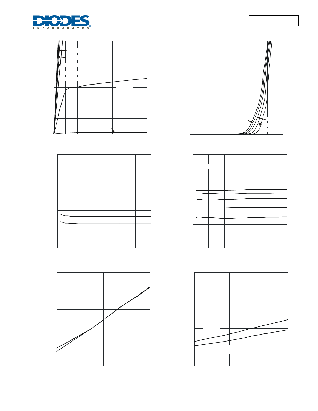
Fig. 1 Typical Output C har acteristic
0.020
Ω
E ( )
10
D
-I , D
5
T = 150°C
A
T = 125°C
A
0
0 0.5 1 1.5 2 2.5 3
-V , GATE-SOURCE VOLT AGE (V)
GS
Fig. 2 Typic al Transfer Characteristi c
0.016
Ω
E ( )
0.014
V = -4.5V
GS
T = 85°C
A
T = 25°C
A
T = -55°C
A
0.016
0.012
ESIS
AIN-S
, D
DS(ON)
0.012
0.008
V = -4.5V
GS
V = -10V
0.004
0
0 5 10 15 20 25 30
-I , DRAIN-SOURCE CURRENT (A)
D
Fig. 3 Typical On-Resistance
GS
vs. Drain C urrent an d G at e Vol tage
1.6
ESIS
0.010
0.008
0.006
AIN-S
0.004
, D
0.002
DS(ON)
0
0 5 10 15 20 25 30
-I , DRAIN CURRENT (A)
D
T = 150°C
A
T = 125°C
A
T = 85°C
A
T = 25°C
T = -55°C
Fig. 4 Typical On-Resistance
vs. Drain C urrent an d Temperatu r e
0.020
A
A
1.4
0.016
E
1.2
0.012
AIN-S
V = -4.5V
1.0
V = -10V
GS
I = -20A
DSON
R , DRAIN-SOURCE
D
0.8
ON-RESISTANCE (NORMALIZED)
0.6
-50 -25 0 25 50 75 100 125 150
V = -4.5V
GS
I = -10A
D
T , AMBIENT TEMPERATURE (°C)
A
Fig. 5 On-Resistance Variation with Temperature
, D
0.008
DSON
0.004
ON-RESISTANCE (NORMALIZED)
GS
I = -10A
D
V = -10V
GS
I = -20A
D
0
-50 -25 0 25 50 75 100 125 150
T , JUNCTION TEMPERATURE (°C)
J
Fig. 6 On- Resistance Variati on with Temperature
DMP3010LK3
Document number: DS35716 Rev. 4 - 2
3 of 7
www.diodes.com
February 2012
© Diodes Incorporated
Page 4

OUR
CE CUR
RENT
C
UNC
TION CAPACITANC
F
GE CUR
REN
T
T
OUR
C
OLT
G
G
P, P
T
RAN
N
T
P
O
R
θ
DMP3010LK3
2.5
2.0
30
25
(A)
20
I = -1mA
I = -250µA
D
D
T = 25°C
15
A
1.5
1.0
10
S
0.5
GS(TH)
-V , GATE THRESHOLD VOLTAGE (V)
0
-50 -25 0 25 50 75 100 125 150
T , AMBIENT TEMPERATURE (°C)
A
Fig. 7 Gate Threshold Variation vs. Ambient Temperature
10,000
)
C
iss
E (p
-I , S
5
0
0 0.2 0.4 0.6 0.8 1.0 1.2 1.4
-V , SOURCE-DRAIN VOLTAGE (V)
SD
Fig. 8 Diode Forward Voltage vs. Current
100,000
10,000
(nA)
T = 150°C
A
C
oss
1,000
T = 125°C
A
1,000
C
rss
, J
T
100
f = 1MHz
0 4 8 121620
-V , DRAIN-SOURCE VOLTAGE (V)
DS
Fig. 9 Typical Total Capacitance
10
V = -15V
8
E(V)
DS
I = -10A
D
A
6
E V
4
E-S
GS
2
-V , A
DSS
-I , LEAKA
100
10
1
0 5 10 15 20 25 30
-V , DRAIN-SOURCE VOLTAGE (V)
DS
T = 85°C
A
T = 25°C
A
Fig. 10 Typical Leakage Current vs. Drain-Source Voltage
100
Single Pulse
R = 72°C/W
θ
JA
R (t) = r(t) * R
θθ
JA JA
T - T
= P * R
JA JA
(W)
WE
SIE
90
80
70
60
50
40
30
EAK
20
(pk)
10
0
0 20406080100120140
Q , OTAL GATE CHARGE (nC)
T
g
Fig. 11 Gate-Source Voltage vs. Total Gate Charge
0
0.001 0.01 0.1 1 10 100 1,000
t1, PULSE DURATION TIME (sec)
Fig. 12 Single Pulse Maximum Power Dissipation
DMP3010LK3
Document number: DS35716 Rev. 4 - 2
4 of 7
www.diodes.com
February 2012
© Diodes Incorporated
Page 5

C
C
R
R
NCH
N
R
G
Y
T
R
T T
HER
R
TANC
DMP3010LK3
700
Starting Temperature (T ) = 25°C
J
600
E
(mJ)
500
AS
E
400
E E
I
AS
300
200
AS
E , AVALA
100
0
0.2 0.4 0.6 0.8 1.0
0.1 0.3 0.5 0.7 0.9
80
70
60
50
40
30
20
10
0
I , AVALAN
AS
HE
U
ENT (A)
INDUCTOR (mH)
Fig. 13 Sin gle-Pulse Aval anche Tested
1
D = 0.7
E
D = 0.5
D = 0.3
ESIS
0.1
D = 0.1
MAL
D = 0.50
D = 0.9
D = 0.02
0.01
ANSIEN
r(t),
D = 0.01
D = 0.005
D = Single Pulse
R (t) = r(t) * R
θθ
JA JA
R = 72°C/W
θ
JA
Duty Cycle, D = t1/ t2
0.001
0.001 0.01 0.1 1 10 100 1,000 10,000
t1, PULSE DURATION TIMES (sec)
Fig. 14 Transient Thermal Resistance
DMP3010LK3
Document number: DS35716 Rev. 4 - 2
5 of 7
www.diodes.com
February 2012
© Diodes Incorporated
Page 6

Package Outline Dimensions
2X b2
E
b3
L3
D
H
L4
e
3X b
Suggested Pad Layout
X2
Y2
Y1
X1
E1
DMP3010LK3
Dim Min Max Typ
A
c2
A2
A1
L
a
Z
C
E1
Dimensions Value (in mm)
Z 11.6
X1 1.5
X2 7.0
Y1 2.5
Y2 7.0
C 6.9
E1 2.3
A1 0.00 0.13 0.08
A2 0.97 1.17 1.07
b2 0.76 1.14 0.95
b3 5.21 5.46 5.33
c2 0.45 0.58 0.531
D1 5.21
E1 4.32
L3 0.88 1.27 1.08
L4 0.64 1.02 0.83
TO252
A 2.19 2.39 2.29
b 0.64 0.88 0.783
D 6.00 6.20 6.10
− −
e
− −
E 6.45 6.70 6.58
H 9.40 10.41 9.91
L 1.40 1.78 1.59
a 0° 10°
All Dimensions in mm
2.286
− −
−
DMP3010LK3
Document number: DS35716 Rev. 4 - 2
6 of 7
www.diodes.com
February 2012
© Diodes Incorporated
Page 7

IMPORTANT NOTICE
DIODES INCORPORATED MAKES NO WARRANTY OF ANY KIND, EXPRESS OR IMPLIED, WITH REGARDS TO THIS DOCUMENT,
INCLUDING, BUT NOT LIMITED TO, THE IMPLIED WARRANTIES OF MERCHANTABILITY AND FITNESS FOR A PARTICULAR PURPOSE
(AND THEIR EQUIVALENTS UNDER THE LAWS OF ANY JURISDICTION).
Diodes Incorporated and its subsidiaries reserve the right to make modifications, enhancements, improvements, corrections or other changes
without further notice to this document and any product described herein. Diodes Incorporated does not assume any liability arising out of the
application or use of this document or any product described herein; neither does Diodes Incorporated convey any license under its patent or
trademark rights, nor the rights of others. Any Customer or user of this document o r products described herein in such applica tions shall assume
all risks of such use and will agree to hold Diodes Incorporated and all the companies whose products are represented on Diodes Incorporated
website, harmless against all damages.
Diodes Incorporated does not warrant or accept any liability whatsoever in respect of any products purchased through unauthorized sales channel.
Should Customers purchase or use Diodes Incorporated products for any unintended or unauthorize d application, Customers shall indemnify and
hold Diodes Incorporated and its representatives harmless against all claims, damages, expenses, and attorney fees arising out of, directly or
indirectly, any claim of personal injury or death associated with such unintended or unauthorized application.
Products described herein may be covered by one or more United States, international or foreign patents pending. Product names and markings
noted herein may also be covered by one or more United States, international or foreign trademarks.
LIFE SUPPORT
Diodes Incorporated products are specifically not authorized for use as critical components in life support devices or systems without the express
written approval of the Chief Executive Officer of Diodes Incorporated. As used herein:
A. Life support devices or systems are devices or systems which:
1. are intended to implant into the body, or
2. support or sustain life and whose failure to perform when properly used in accordance with instructions for use provided in the
labeling can be reasonably expected to result in significant injury to the user.
B. A critical component is any component in a life support device or system whose failure to perform can be reasonably expected to cause the
failure of the life support device or to affect its safety or effectiveness.
Customers represent that they have all necessary expertise in the safety and regulatory ramifications of their life support devices or systems, and
acknowledge and agree that they are solely responsible for all legal, regulatory and safety-related requirements concerning their products and any
use of Diodes Incorporated products in such safety-critical, life support devices or systems, notwithstanding any devices- or systems-related
information or support that may be provided by Diodes Incorporated. Further, Customers must fully indemnify Diodes Incorporated and its
representatives against any damages arising out of the use of Diodes Incorporated products in such safety-critical, life support devices or systems.
Copyright © 2012, Diodes Incorporated
www.diodes.com
DMP3010LK3
DMP3010LK3
Document number: DS35716 Rev. 4 - 2
7 of 7
www.diodes.com
February 2012
© Diodes Incorporated
 Loading...