Diodes DMP21D0UT User Manual

A
f
Product Summary
I
Max
D
V
(BR)DSS
-20V
R
495mΩ @ V
690mΩ @ VGS = -2.5V
960mΩ @ VGS = -1.8V
DS(on)
Max
= -4.5V
GS
@ TA = 25°C
(Note 4)
-0.59A
-0.50A
-0.42A
Description and Applications
This MOSFET has been designed to minimize the on-state resistance
(R
) and yet maintain superior switching performance, making it
DS(on)
ideal for high efficiency power management applications.
• Portable electronics
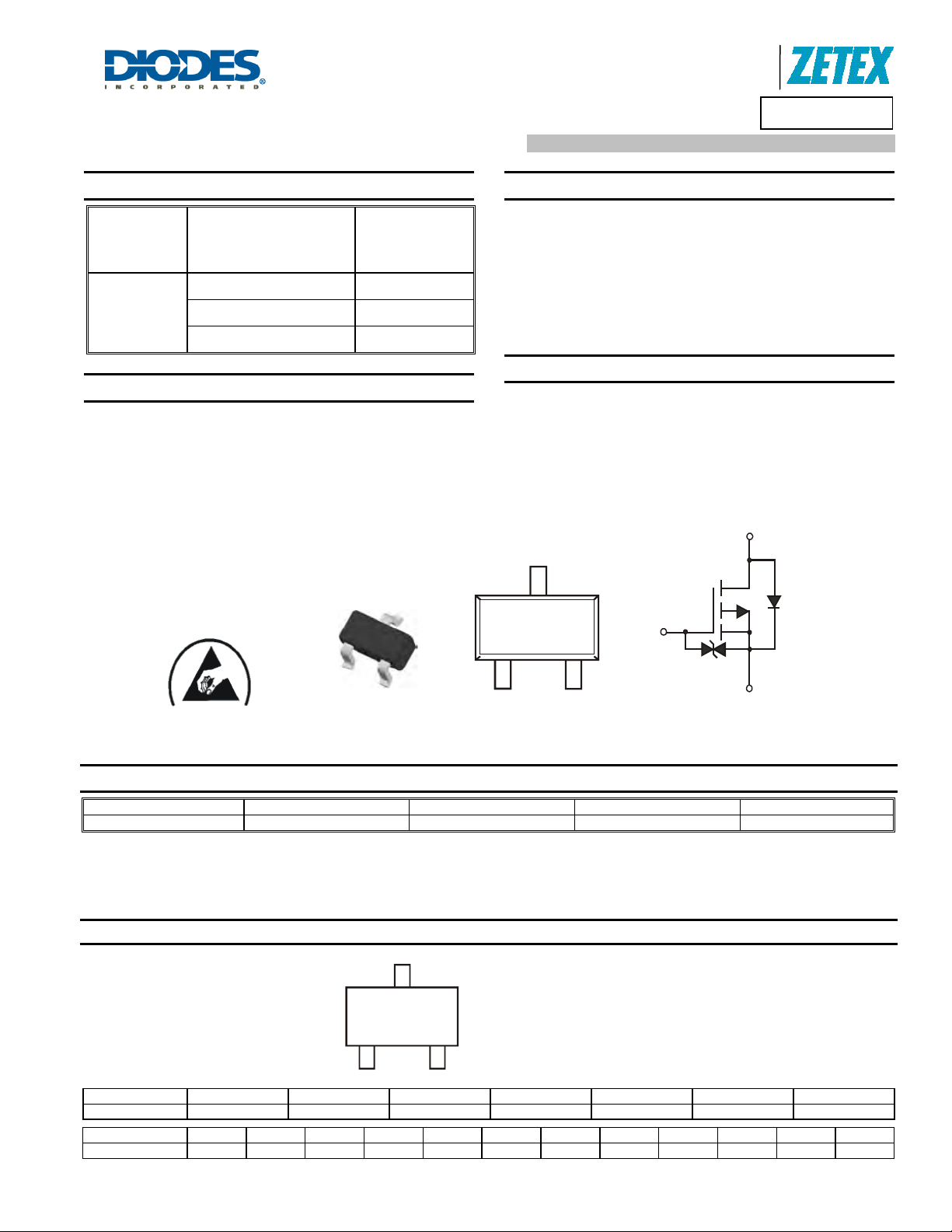
ESD PROTECTED TO 3kV
SOT523
Bottom View
Product Line o
Diodes Incorporated
DMP21D0UT
20V P-CHANNEL ENHANCEMENT MODE MOSFET
Features and Benefits
• Footprint of just 3mm2 – less than half the size of SOT23
• 0.8mm profile – ideal for low profile applications
• Low Gate Threshold Voltage
• Fast Switching Speed
• ESD Protected Gate 3KV
• Totally Lead-Free & Fully RoHS compliant (Note 1)
• Halogen and Antimony Free. “Green” Device (Note 2)
• Qualified to AEC-Q101 Standards for High Reliability
Mechanical Data
• Case: SOT523
• Case Material: Molded Plastic, “Green” Molding Compound.
UL Flammability Classification Rating 94V-0
• Moisture Sensitivity: Level 1 per J-STD-020
• Terminals: Matte Tin Finish ; Solderable per MIL-STD-202,
Method 208
• Weight: 0.002 grams (approximate)
Drain
D
Gate
G
Internal Schematic
S
Gate
Protection
Diode
Equivalent CircuitTop View
Source
Ordering Information (Note 3)
Part Number Marking Reel size (inches) Tape width (mm) Quantity per reel
DMP21D0UT-7 PBC 7 8 3,000
Notes: 1. EU Directive 2002/95/EC (RoHS) & 2011/65/EU (RoHS 2) compliant. No purposely added lead. Halogen and Antimony free.
2. Diodes Inc's "Green" policy can be found on our website at http://www.diodes.com.
3. For packaging details, go to our website at http://www.diodes.com.
Marking Information
Date Code Key
Year 2011 2012 2013 2014 2015 2016 2017
Code Y Z A B C D E
Month Jan Feb Mar Apr May Jun Jul Aug Sep Oct Nov Dec
Code 1 2 3 4 5 6 7 8 9 O N D
DMP21D0UT
D
atasheet Number: DS35297 Rev. 2 - 2
PBC
YM
www.diodes.com
PBC = Product Type Marking Code
YM = Date Code Marking
Y = Year (ex: Y = 2011)
M = Month (ex: 9 = September)
1 of 7
March 2012
© Diodes Incorporated

A
f
P
P
T
R
T P
OWER
T
R
T T
HER
R
TANC
Maximum Ratings @T
= 25°C unless otherwise specified
A
Characteristic Symbol Value Unit
Drain-Source Voltage
Gate-Source Voltage
Continuous Drain Current
Pulsed Drain Current (Note 6)
Steady
State
= 25°C (Note 4)
T
A
= 85°C (Note 4)
T
A
T
= 25°C (Note 5)
A
V
V
DSS
GSS
I
I
DM
D
Thermal Characteristics @T
= 25°C unless otherwise specified
A
Characteristic Symbol Value Unit
Power Dissipation (Note 4)
Power Dissipation (Note 5)
Thermal Resistance, Junction to Ambient (Note 4)
Thermal Resistance, Junction to Ambient (Note 5)
Operating and Storage Temperature Range
Notes: 4. Device mounted on FR-4 substrate PC board, 2oz copper, with minimum recommended pad layout
5. Device mounted on 25mm X 25mm FR-4 PCB with high coverage of 2oz copper
6. Device mounted on minimum recommended pad layout test board, 10μs pulse duty cycle = 1%.
P
D
P
D
R
θJA
R
θJA
T
, T
J
STG
10
9
(W)
8
7
Product Line o
Diodes Incorporated
DMP21D0UT
-20 V
±8 V
-0.59
-0.42
-0.65
-5.0 A
0.24 W
0.33 W
525 °C/W
383 °C/W
-55 to +150 °C
Single Pulse
R = 380°C/W
θ
JA
R (t) = r(t) * R
θθ
JA JA
T - T = P * R (t)
JA JA
θ
A
6
5
ANSIEN
4
3
EAK
2
(pk),
1
0
0.0001 0.001 0.01 0.1 1 10 100 1,000
t , PULSE DURA TION TIME (SEC)
1
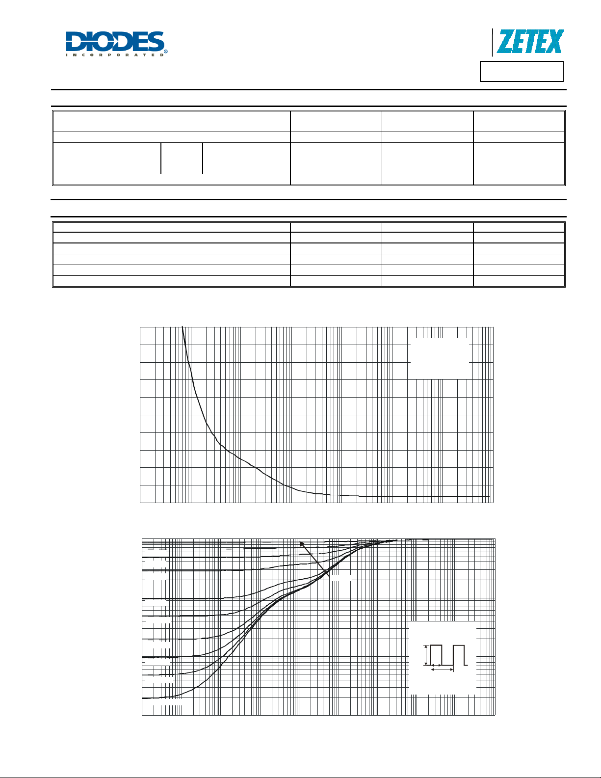
Fig. 1 Single Pulse Maximum Power Dissipation
1
D = 0.7
E
D = 0.5
D = 0.3
ESIS
0.1
D = 0.1
MAL
D = 0.05
D = 0.02
0.01
D = 0.01
ANSIEN
D = 0.005
r(t),
D = Single Pulse
0.001
0.000001 0.00001 0.0001 0.001 0.01 0.1 1 10 100 1,000
DMP21D0UT
D
atasheet Number: DS35297 Rev. 2 - 2
t , PULSE DURA TION TIME (s)
1
Fig. 2 Transient Thermal Response
www.diodes.com
2 of 7
D = 0.9
R (t) = r(t) *
θ
JA
R = 380°C/W
JA
P(pk)
t
1
t
2
T - T = P * R (t)
JA JA12θ
Duty Cycle, D = t /t
R
θθJA
March 2012
© Diodes Incorporated

A
f
)
g
g
g
g
g
)
r
)
R
C
U
R
R
T
R
N C
U
R
REN
T
Electrical Characteristics @T
= 25°C unless otherwise specified
A
Characteristic Symbol Min Typ Max Unit Test Condition
OFF CHARACTERISTICS (Note 7)
Drain-Source Breakdown Voltage
Zero Gate Voltage Drain Current TJ = 25°C I
Gate-Source Leakage
ON CHARACTERISTICS (Note 7)
Gate Threshold Voltage
Static Drain-Source On-Resistance
Forward Transfer Admittance
Diode Forward Voltage
DYNAMIC CHARACTERISTICS
Input Capacitance
Output Capacitance
Reverse Transfer Capacitance
Gate Resistance
Total Gate Charge
Total Gate Charge
Gate-Source Charge
Gate-Drain Charge
Turn-On Delay Time
Turn-On Rise Time
Turn-Off Delay Time
Turn-Off Fall Time
Notes: 7. Short duration pulse test used to minimize self-heating effect.
2.0
1.5
(A)
V = -4.5V
GS
V = -4.0V
GS
V = -3.0V
GS
V = -2.5V
GS
V = -2.0V
GS
EN
V = -1.8V
1.0
GS
BV
I
V
GS(th
R
DS (ON)
|Y
V
C
C
C
Q
Q
t
D(on
t
D(off
DSS
DSS
GSS
SD
iss
oss
rss
R
Q
Q
t
t
Product Line o
Diodes Incorporated
DMP21D0UT
-20 - - V
- - -1
- - ±10
- -0.7 - V
495
- -
690
960
fs
s
d
f
- - -1.2 V
-
76.5
-
13.7
-
10.7
-
-
-
-
-
-
-
-
195
1.5
1.0
0.2
0.3
7.1
8.0
31.7
18.5
-
-
-
-
-
-
-
-
-
-
-
-
50 - - mS
|
2.0
V = -5V
1.5
DS
(A)
1.0
VGS = 0V, ID = -250μA
μA
VDS = -20V, VGS = 0V
μA
VGS = ±8V, VDS = 0V
VDS = VGS, ID = -250μA
= -4.5V, ID = -400mA
V
GS
mΩ
V
= -2.5V, ID = -300mA
GS
V
= -1.8V, ID = -100mA
GS
VDS = -3V, ID = -300mA
VGS = 0V, IS = -300mA
pF
V
= -10V, VGS = 0V,
pF
pF
nC
nC
nC
nC
DS
f = 1.0MHz
Ω
VDS = 0V, VGS = 0V, f = 1MHz
VGS = -8V,VDS = -15V,ID = -1A
V
= -4.5V, VDS = -15V,
GS
I
= -1A
D
ns
ns
V
= -10V, -I
ns
DS
= -4.5V, RG = 6Ω
V
GS
ns
= 1A
D
AIN
D
-I , D
0.5
0
012345
-V , DRAIN-SOURCE VOLTAGE (V)
DS
V = -1.5V
GS
V = -1.2V
GS
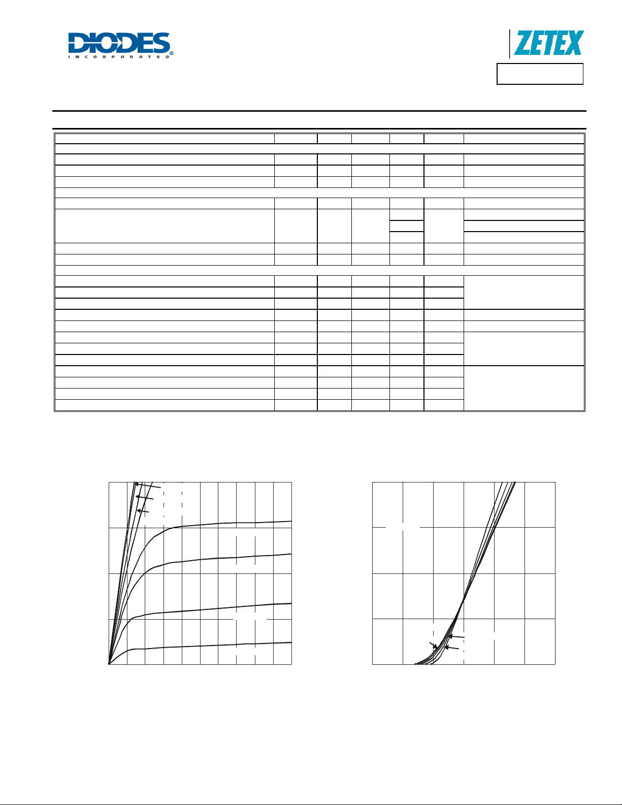
Fig. 3 Typical Output C har acterist ic
AI
D
-I , D
0.5
0
0 0.5 1.0 1.5 2.0 2.5 3.0
T = 150°C
A
T = 125°C
A
-V , GATE-SOURCE VOLTAGE (V)
GS
Fig. 4 Typical Transfer Characteristic
T = 85°C
A
T = 25°C
A
T = -55°C
A
DMP21D0UT
D
atasheet Number: DS35297 Rev. 2 - 2
3 of 7
www.diodes.com
March 2012
© Diodes Incorporated
 Loading...