Diodes DMP21D0UFD User Manual

A
f
Product Line o
Diodes Incorporated
DMP21D0UFD
20V P-CHANNEL ENHANCEMENT MODE MOSFET
Product Summary
V
(BR)DSS
-20V
R
495mΩ @ V
730mΩ @ VGS = -2.5V
960mΩ @ VGS = -1.8V
1300mΩ @ VGS = -1.5V
Description and Applications
This MOSFET has been designed to minimize the on-state resistance
(R
) and yet maintain superior switching performance, making it
DS(on)
ideal for high efficiency power management applications.
• Portable electronics
ESD PROTECTED TO 3kV
DS(on)
Max
= -4.5V
GS
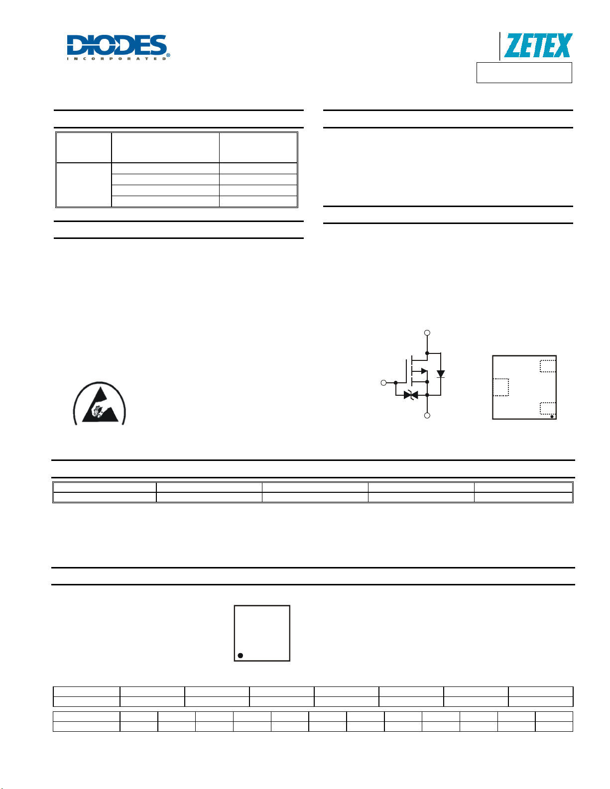
X1-DFN1212-3
Top View Bottom View
max
I
D
= 25°C
T
A
(Notes 4)
-1.14A
-0.94A
-0.85A
-0.75A
Features and Benefits
• Low Gate Threshold Voltage
• Fast Switching Speed
• ESD Protected Gate 3KV
• Totally Lead-Free & Fully RoHS compliant (Note 1)
• Halogen and Antimony Free. “Green” Device (Note 2)
• Qualified to AEC-Q101 Standards for High Reliability
Mechanical Data
• Case: X1-DFN1212-3
• Case Material: Molded Plastic, “Green” Molding Compound.
UL Flammability Classification Rating 94V-0
• Moisture Sensitivity: Level 1 per J-STD-020
• Terminals: Finish – NiPdAu over Copper leadframe. Solderable
per MIL-STD-202, Method 208
• Weight: 0.005 grams (approximate)
Drain
Gate
D
Gate
Protection
Diode
Equivalent Circuit
Source
Pin-out Top view
S
G
Ordering Information (Note 3)
Part Number Marking Reel size (inches) Tape width (mm) Quantity per reel
DMP21D0UFD-7 K21 7 8 3000
Notes: 1. No purposely added lead. Fully EU Directive 2002/95/EC (RoHS) & 2011/65/EU (RoHS 2) compliant.
3. For packaging details, go to our website at http://www.diodes.com.
2. Halogen and Antimony free "Green” products are defined as those which contain <900ppm bromine, <900ppm chlorine (<1500ppm total Br + Cl) and
<1000ppm antimony compounds.
Marking Information
Date Code Key
Year 2011 2012 2013 2014 2015 2016 2017
Code Y Z A B C D E
Month Jan Feb Mar Apr May Jun Jul Aug Sep Oct Nov Dec
Code 1 2 3 4 5 6 7 8 9 O N D
K21
YM
DMP21D0UFD
Datasheet Number: DS35364
Rev. 4 - 2
K21 = Product Type Marking Code
YM = Date Code Marking
Y = Year (ex: Y = 2011)
M = Month (ex: 9 = September)
1 of 8
www.diodes.com
March 2012
© Diodes Incorporated

A
f
Product Line o
Diodes Incorporated
DMP21D0UFD
Maximum Ratings @T
= 25°C unless otherwise specified
A
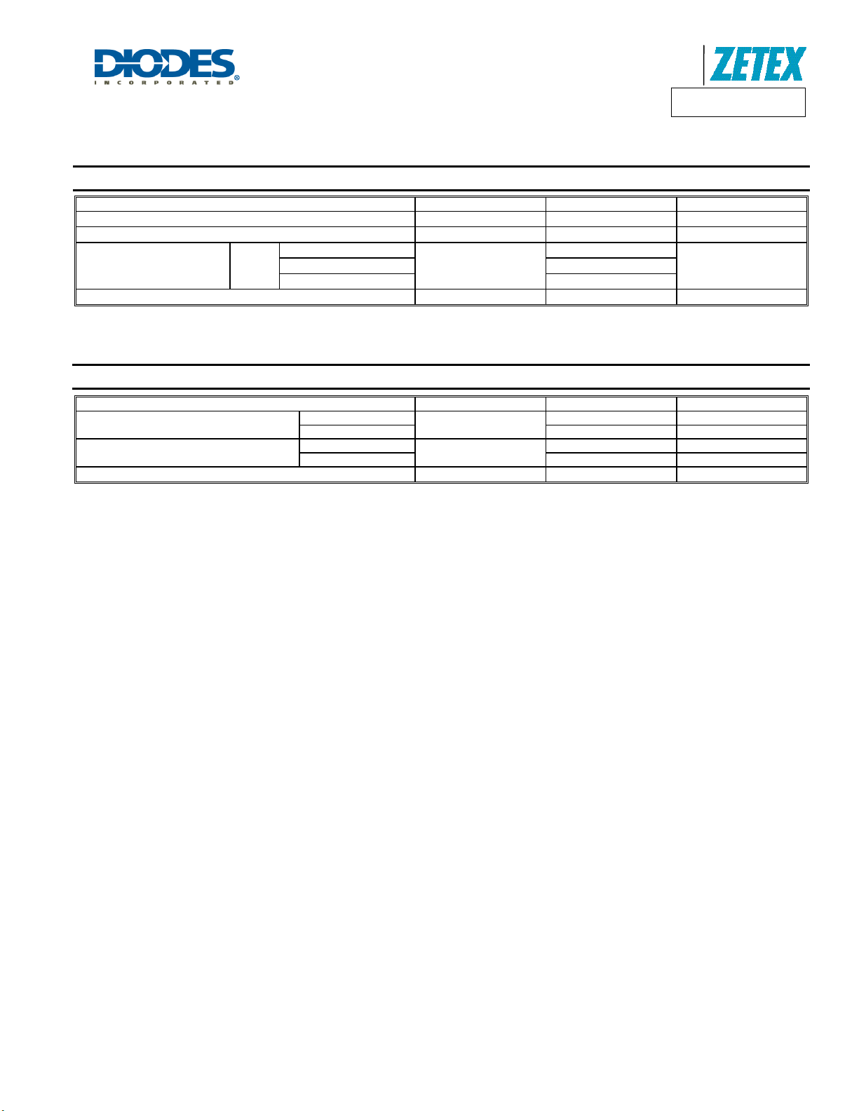
Characteristic Symbol Value Unit
Drain-Source Voltage
Gate-Source Voltage
Continuous Drain Current
Pulsed Drain Current (Note 6)
Steady
State
T
= 25°C (Note 4)
A
T
= 85°C (Note 4)
A
T
= 25°C (Note 5)
A
V
V
DSS
GSS
I
I
DM
D
-20 V
±8 V
-1.14
-0.83
A
-0.82
-4.0 A
Thermal Characteristics @T
= 25°C unless otherwise specified
A
Characteristic Symbol Value Unit
Power Dissipation
Thermal Resistance, Junction to Ambient
Operating and Storage Temperature Range
Notes: 4. For a device surface mounted on 15mm x 15mm x 1.6mm FR4 PCB with high coverage of 2oz copper, in still air conditions; the device is measured
when operating in a steady-state condition.
5. Same as note 4, except the device is mounted on minimum recommended pad layout.
6. Device mounted on minimum recommended pad layout test board, 10µs pulse duty cycle = 1%.
(Note 4)
(Note 5) 490 mW
(Note 4)
(Note 5) 256 °C/W
P
D
R
θJA
T
, T
J
STG
930 mW
135 °C/W
-55 to +150 °C
DMP21D0UFD
Datasheet Number: DS35364
Rev. 4 - 2
2 of 8
www.diodes.com
March 2012
© Diodes Incorporated

A
f
θ
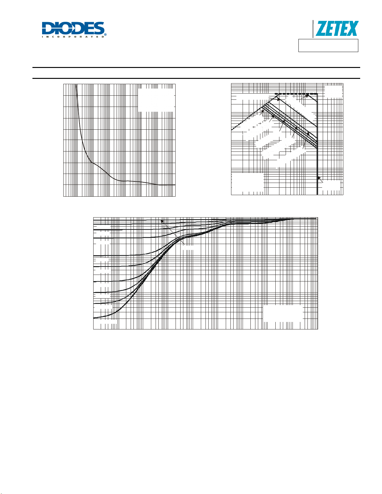
Thermal Characteristics
10
9
8
7
6
5
4
3
2
P(pk), PEAK TRANSIENT POWER (W)
1
0
0.0001 0.001 0.01 0.1 1 10 100 1000
t1, PULSE DURATION TIME (sec)
Fig. 1 Single Pulse Maximum Power Dissipation
1
D = 0.7
D = 0.5
D = 0.3
0.1
D = 0.1
Single Pulse
R = 136 C/W
R (t) = R *r(t)
T - T = P*R
°
θ
JA
θθ
JA JA
JA JA
D = 0.9
Product Line o
Diodes Incorporated
DMP21D0UFD
10
-I (A) @P =1ms
DW
I , DRAIN CURRENT (A)
D
0.01
1
0.1
T = 150 C
T= 25C
Single Puls e
-
J(MAX)
A
C
D
@
)
A
(
I
D
I
-
°
0
1
=
W
P
@
)
A
(
D
P
@
)
A
(
I
-
D
A
(
I
-
D
°
0.001
0.1 1 10 100
-V , DRAIN-SOURCE VOLTAGE (V)
DS
Fig. 2 SOA, Safe Oper ation Area
-
I
D
(
A
)
@
P
W
=
1
0
0
µ
s
s
s
1
=
W
s
m
0
0
1
=
W
P
@
)
A
(
I
-
D
s
m
0
1
=
W
P
@
)
R
DS(ON)
Limited
-I (A) @
D
P =10µs
W
D = 0.05
D = 0.02
0.01
D = 0.01
r(t), TRANSIENT THERMAL RESISTANCE
0.001
D = 0.005
Single Puls e
0.000001
0.00001 0.0001 0.001 0.01 0.1 1 10 100 1,000
R (t) = r(t) * R
θθJA
R = 54°C/W
JA
Duty Cycle, D =t1/ t2
θ
JA
t1, PULSE DURATION TIMES (sec)
Fig. 3 Transient Therm al Resist ance
DMP21D0UFD
Datasheet Number: DS35364
Rev. 4 - 2
3 of 8
www.diodes.com
March 2012
© Diodes Incorporated
 Loading...