Diodes DMN4036LK3 User Manual

A
f
D
Product Summary
I
V
R
(BR)DSS
40V
DS(on)
36mΩ @ V
61mΩ @ VGS= 4.5V
GS
= 10V
T
= 25°C
A
12.2A
9.4A
D
Description and Applications
This MOSFET has been designed to minimize the on-state resistance
) and yet maintain superior switching performance, making it
(R
DS(on)
ideal for high efficiency power management applications.
• Backlighting
• DC-DC Converters
• Power management functions
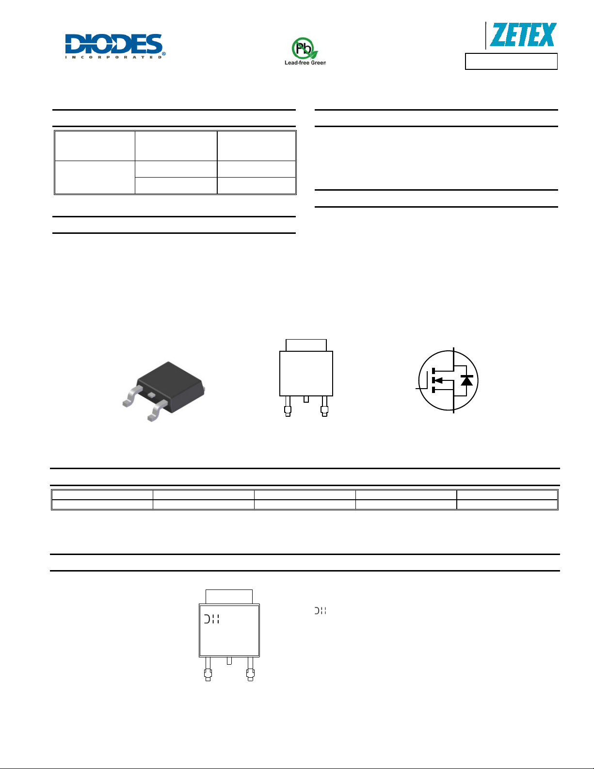
TO252-3L
TOP VIEW PIN OUT -TOP VIEW
40V N-CHANNEL ENHANCEMENT MODE MOSFET
Features and Benefits
• Low on-resistance
• Fast switching speed
• “Green” component and RoHS compliant (Note 1)
• Qualified to AEC-Q101 Standards for High Reliability
Mechanical Data
• Case: TO252-3L
• Case Material: Molded Plastic, “Green” Molding Compound.
UL Flammability Classification Rating 94V-0 (Note 1)
• Moisture Sensitivity: Level 1 per J-STD-020
• Terminals Connections: See Diagram
• Terminals: Matte Tin Finish annealed over Copper leadframe.
Solderable per MIL-STD-202, Method 208
• Weight: 0.33 grams (approximate)
D
GS
Product Line o
Diodes Incorporated
D
G
S
Equivalent Circuit
DMN4036LK3
Ordering Information (Note 1)
Product Marking Reel size (inches) Tape width (mm) Quantity per reel
DMN4036LK3-13 N4036L 13 16 2,500
Note: 1. Diodes, Inc. defines “Green” products as those which are RoHS compliant and contain no halogens or antimony compounds; further information about
Diodes Inc.’s “Green” Policy can be found on our website. For packaging details, go to our website.
Marking Information
DMN4036LK3
Document number: DS32122 Rev. 2 - 2
= Manufacturer’s Marking
YYWW
N4036L
www.diodes.com
N4036L = Product Type Marking Code
YYWW = Date Code Marking
YY = Year (ex: 09 = 2009)
WW = Week (01 - 53)
1 of 8
March 2010
© Diodes Incorporated

A
f
θ
Product Line o
Diodes Incorporated
DMN4036LK3
Maximum Ratings @T
= 25°C unless otherwise specified
A
Characteristic Symbol Value Unit
Drain-Source voltage
Gate-Source voltage (Note 2)
(Note 4)
Continuous Drain current
V
= 10V
GS
TA = 70°C (Note 4)
(Note 3) 8.5
Pulsed Drain current
V
= 10V
GS
(Note 5)
Continuous Source current (Body diode) (Note 4)
Pulsed Source current (Body diode) (Note 5)
Thermal Characteristics @T
= 25°C unless otherwise specified
A
Characteristic Symbol Value Unit
(Note 3)
Power dissipation
Linear derating factor
(Note 4)
(Note 6)
(Note 3)
Thermal Resistance, Junction to Ambient
(Note 4) 14.7
(Note 6) 59.0
Thermal Resistance, Junction to Lead (Note 7)
Operating and storage temperature range
Notes: 2. AEC-Q101 VGS maximum is ±16V.
3. For a device surface mounted on 50mm x 50mm x 1.6mm FR4 PCB with high coverage of single sided 2oz copper, in still air conditions; the device is
measured when operating in a steady-state condition.
4. Same as note 3, except the device is measured at t ≤ 10 sec.
5. Same as note 3, except the device is pulsed with D = 0.02 and pulse width 300 µs. The pulse current is limited by the maximum junction temperature.
6. For a device surface mounted on 25mm x 25mm x 1.6mm FR4 PCB with high coverage of single sided 1oz copper, in still air conditions; the device is
measured when operating in a steady-state condition.
7. Thermal resistance from junction to solder-point (at the end of the drain lead).
V
DSS
V
GS
40 V
±20
V
12.2
I
D
IDM
I
S
I
SM
9.7
31.7 A
10.4 A
31.7 A
A
4.12
33
P
D
8.49
67.9
W
mW/°C
2.12
16.9
30.3
R
JA
θ
R
JL
T
, T
J
STG
3.1
-55 to 150
°C/W
°C
DMN4036LK3
Document number: DS32122 Rev. 2 - 2
2 of 8
www.diodes.com
March 2010
© Diodes Incorporated

A
f
Thermal Characteristics
Product Line o
Diodes Incorporated
DMN4036LK3
R
DS(on)
Limited
10
DC
100m
Drain Current (A)
D
I
1
1s
100ms
T
=25°C
amb
25mm x 25mm
1oz FR4
110
10ms
1ms
100µs
VDS Drain-Source Voltage (V)
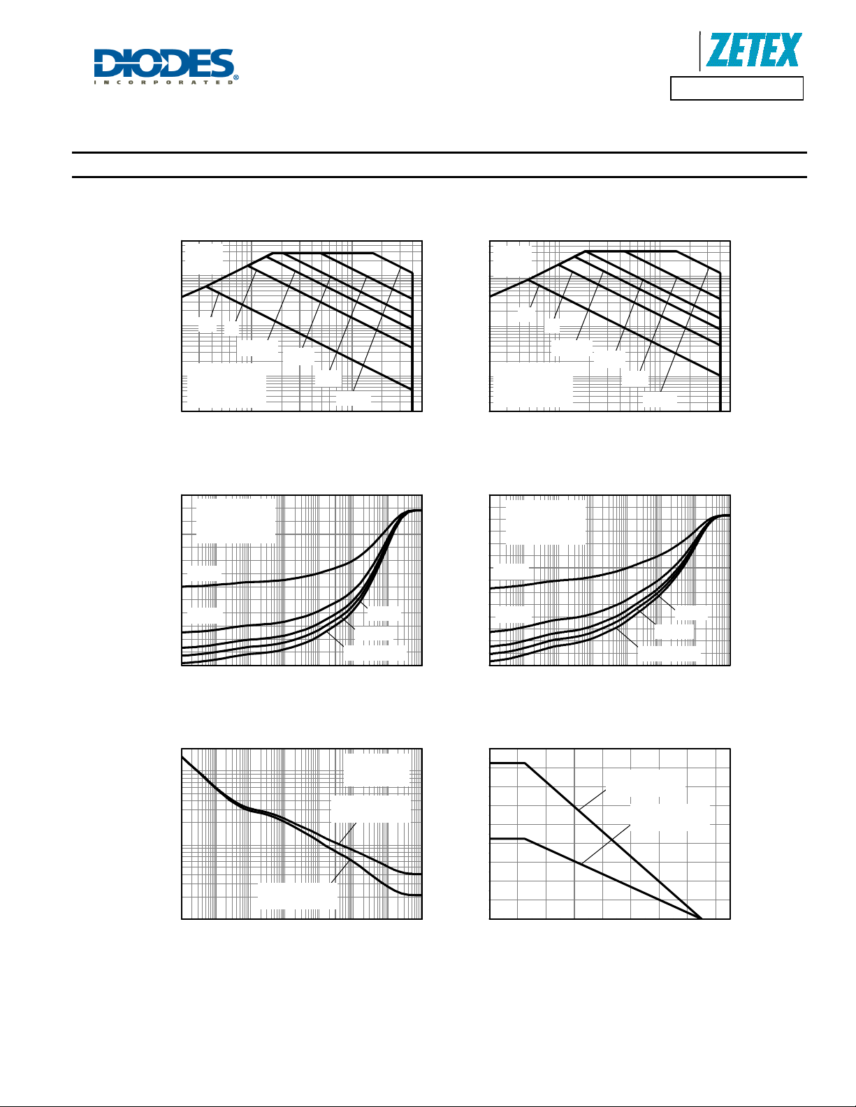
Safe Operating Area
T
60
50
40
30
20
10
0
100µ 1m 10m 100m 1 10 100 1k
Thermal Resistance (°C/W)
=25°C
amb
25mm x 25mm
1oz FR4
D=0.5
D=0.2
D=0.1
D=0.05
Single Pulse
Pulse Width ( s)
Transient Thermal Impedance
R
DS(on)
Limited
10
DC
100m
Drain Current (A)
D
I
1
50mm x 50mm
T
=25°C
amb
2oz FR4
1s
100ms
10ms
1ms
100µs
110
VDS Drain-Sou rce Voltage (V)
Safe Operating Area
35
30
25
20
15
10
5
0
100µ 1m 10m 100m 1 10 100 1k
Thermal Resistance (°C/W)
T
=25°C
amb
50mm x 50mm
2oz FR4
D=0.5
D=0.2
D=0.1
D=0.05
Single Pulse
Pulse Width (s)
Transient Thermal Impedance
100
10
25mm x 25mm
1oz FR4
1
100µ 1m 10m 100m 1 10 100 1k
Max Power Dissipation (W)
Pulse Width (s)
Single Pulse
T
=25°C
amb
50mm x 50mm
2oz FR4
Pulse Power Dissipation
4.5
4.0
3.5
3.0
2.5
2.0
1.5
1.0
0.5
0.0
0 20 40 60 80 100 120 140 160
Max Power Dissipation (W)
Temperature (°C)
50mm x 50mm
2oz FR4
25mm x 25mm
1oz FR4
Derating Curve
DMN4036LK3
Document number: DS32122 Rev. 2 - 2
3 of 8
www.diodes.com
March 2010
© Diodes Incorporated
 Loading...