Diodes DMN4010LFG User Manual

DMN4010LFG
40V N-CHANNEL ENHANCEMENT MODE MOSFET
POWERDI
®
Product Summary
I
max
D
11.5A
10.3A
V
(BR)DSS
40V
R
12mΩ @ V
15mΩ @ VGS = 4.5V
DS(ON)
max
= 10V
GS
TA = +25°C
Description and Applications
This MOSFET has been designed to minimize the on-state resistance
(R
) and yet maintain superior switching performance, making it
DS(ON)
ideal for high efficiency power management applications.
• Backlighting
• Power Management Functions
• DC-DC Converters
ADVANCE INFORMATION
D
D
D
D
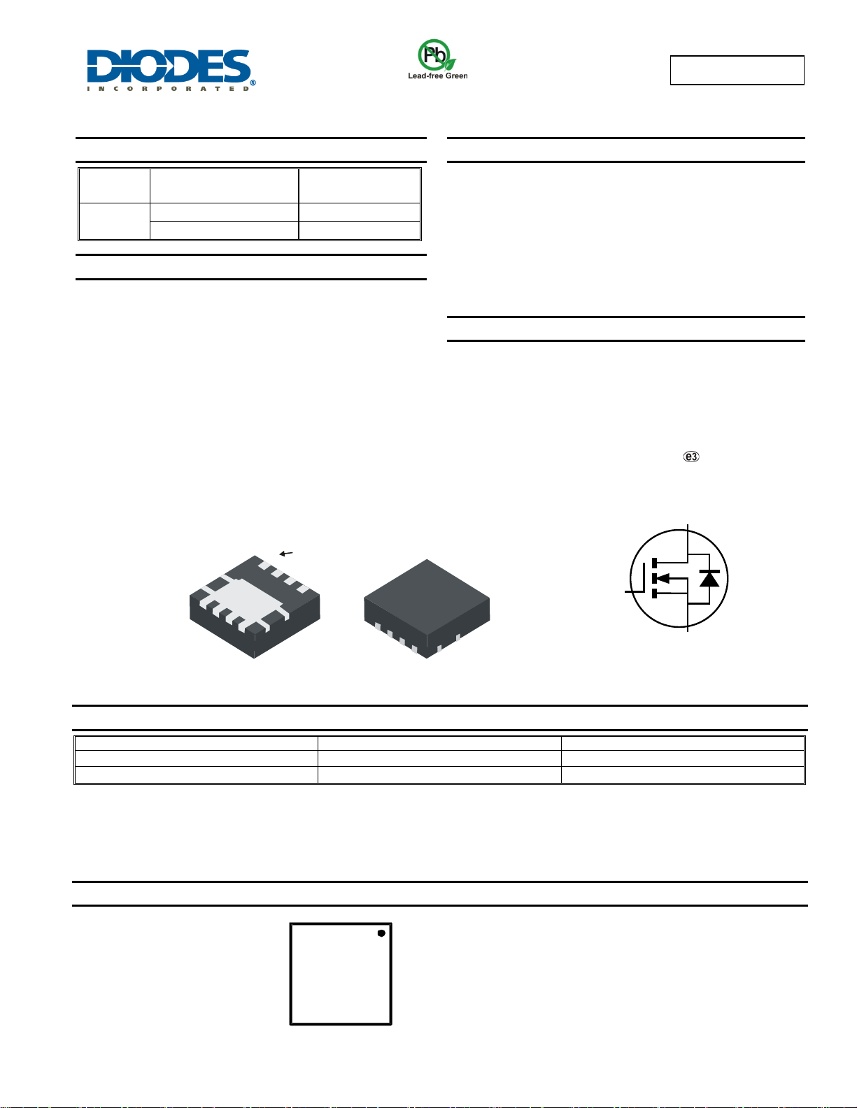
POWERDI 3333-8
Pin 1
S
S
S
G
Features and Benefits
• Low R
• Small form factor thermally efficient package enables higher
density end products
• Occupies just 33% of the board area occupied by SO-8 enabling
smaller end product
• Totally Lead-Free & Fully RoHS Compliant (Notes 1 & 2)
• Halogen and Antimony Free. “Green” Device (Note 3)
• Qualified to AEC-Q101 Standards for High Reliability
– ensures on state losses are minimized
DS(ON)
Mechanical Data
• Case: POWERDI 3333-8
• Case Material: Molded Plastic, "Green" Molding Compound.
UL Flammability Classification Rating 94V-0
• Moisture Sensitivity: Level 1 per J-STD-020
• Terminal Connections Indicator: See diagram
• Terminals: Finish ⎯ Matte Tin annealed over Copper leadframe.
Solderable per MIL-STD-202, Method 208
• Weight: 0.072 grams (approximate)
D
G
S
Top View Bottom View
Equivalent Circuit
Ordering Information (Note 4)
Part Number Case Packaging
DMN4010LFG-7
DMN4010LFG-13
Notes: 1. No purposely added lead. Fully EU Directive 2002/95/EC (RoHS) & 2011/65/EU (RoHS 2) compliant.
2. See http://www.diodes.com/quality/lead_free.html for more information about Diodes Incorporated’s definitions of Halogen- and Antimony-free, "Green"
and Lead-free.
3. Halogen- and Antimony-free "Green” products are defined as those which contain <900ppm bromine, <900ppm chlorine (<1500ppm total Br + Cl) and
<1000ppm antimony compounds.
4. For packaging details, go to our website at http”//www.diodes.com/products/packages.html.
POWERDI 3333-8
POWERDI
3333-8
2000/Tape & Reel
3000/Tape & Reel
Marking Information
POWERDI is a registered trademark of Diodes Incorporated
DMN4010LFG
Document number: DS36764 Rev. 1 - 2
N41= Product Type Marking Code
YYWW = Date Code Marking
YY = Last digit of year (ex: 13 = 2013)
YYWW
WW = Week code (01 ~ 53)
N41
1 of 7
www.diodes.com
April 2014
© Diodes Incorporated

DMN4010LFG
Maximum Ratings (@T
= +25°C, unless otherwise specified.)
A
Characteristic Symbol Value Units
Drain-Source Voltage
Gate-Source Voltage
Steady
Continuous Drain Current (Note 6) VGS = 10V
State
t<10s
Pulsed Drain Current (10μs pulse, duty cycle = 1%)
Maximum Continuous Body Diode Forward Current (Note 6)
Avalanche Current (Note 7) L = 0.1mH
Avalanche Energy (Note 7) L = 0.1mH
= +25°C
T
A
= +70°C
T
A
T
= +25°C
A
= +70°C
T
A
V
DSS
V
GSS
I
D
I
D
I
DM
I
S
I
AS
E
AS
40 V
±20 V
11.5
9.2
14.2
11.4
A
A
2 A
80 A
27 A
37 mJ
Thermal Characteristics (@T
ADVANCE INFORMATION
Total Power Dissipation (Note 5)
Thermal Resistance, Junction to Ambient (Note 5)
Total Power Dissipation (Note 6)
Thermal Resistance, Junction to Ambient (Note 6)
Thermal Resistance, Junction to Case (Note 6)
Operating and Storage Temperature Range
Notes: 5. Device mounted on FR-4 PC board, with minimum recommended pad layout, single sided.
6. Device mounted on FR-4 substrate PC board, 2oz copper, with thermal bias to bottom layer 1inch square copper plate
7. I
and EAS rating are based on low frequency and duty cycles to keep TJ = 25°C
AS
= +25°C, unless otherwise specified.)
A
Characteristic Symbol Value Units
P
D
Steady state
t<10s 89
Steady state
t<10s 34
R
P
R
R
T
J, TSTG
JA
θ
D
JA
θ
JC
θ
0.93 W
137
°C/W
2.45 W
52
°C/W
3
-55 to +150 °C
POWERDI is a registered trademark of Diodes Incorporated
DMN4010LFG
Document number: DS36764 Rev. 1 - 2
2 of 7
www.diodes.com
April 2014
© Diodes Incorporated

R
CUR
RENT
R
C
URR
T
DMN4010LFG
Electrical Characteristics (@T
= +25°C, unless otherwise specified.)
A
Characteristic Symbol Min Typ Max Unit Test Condition
OFF CHARACTERISTICS (Note 8)
Drain-Source Breakdown Voltage
Zero Gate Voltage Drain Current TJ = +25°C I
Gate-Source Leakage
BV
DSS
I
GSS
DSS
40 — — V
— — 1 µA
— — ±100 nA
VGS = 0V, ID = 250μA
VDS = 32V, VGS = 0V
VGS = ±20V, VDS = 0V
ON CHARACTERISTICS (Note 8)
Gate Threshold Voltage
Static Drain-Source On-Resistance
Diode Forward Voltage
V
GS(th)
R
DS (ON)
V
SD
1.0 — 3.0 V
— — 12
— 15
— 0.72 — V
VDS = VGS, ID = 250μA
= 10V, ID = 14A
V
mΩ
GS
V
= 4.5V, ID = 11A
GS
VGS = 0V, IS = 14A
DYNAMIC CHARACTERISTICS (Note 9)
Input Capacitance
Output Capacitance
Reverse Transfer Capacitance
ADVANCE INFORMATION
Gate Resistance
Total Gate Charge (VGS = 4.5V) Qg
C
iss
C
oss
C
rss
R
g
Total Gate Charge (VGS = 10V) Qg
Gate-Source Charge
Gate-Drain Charge
Turn-On Delay Time
Turn-On Rise Time
Turn-Off Delay Time
Turn-Off Fall Time
Body Diode Reverse Recovery Time
Body Diode Reverse Recovery Charge
Notes: 8. Short duration pulse test used to minimize self-heating effect.
9. Guaranteed by design. Not subject to product testing.
Q
Q
t
D(on)
t
t
D(off)
t
Q
gs
gd
r
t
f
rr
rr
—
—
—
— 1.7 —
1810
135
112
— 17 —
— 37 —
— 5.6 —
— 7.1 —
—
—
—
—
— 12.2 — nS
— 5.4 — nC
5.1
13
36
13
—
—
—
pF
VDS = 20V, VGS = 0V,
pF
f = 1.0MHz
pF
Ω
VDS = 0V, VGS = 0V, f = 1MHz
nC
nC
V
DS
nC
nC
— ns
— ns
— ns
V
GS
R
G
— ns
IF = 3A, di/dt = 100A/μs
IF = 3A, di/dt = 100A/μs
= 20V, ID = 14A
= 10V, VDS = 20V,
= 6Ω, ID = 14A
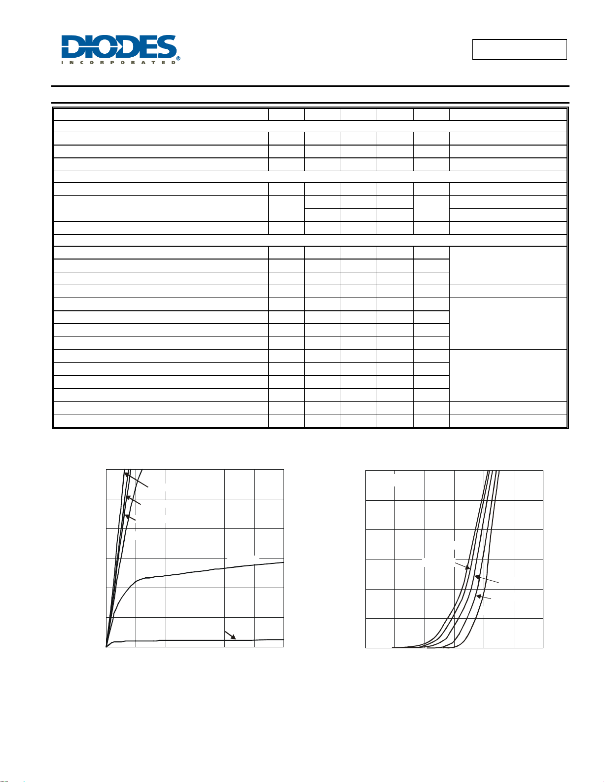
30.0
V = 10VGS
25.0
(A)
20.0
15.0
V= 4.5V
GS
V= 4.0V
GS
V= 3.5V
GS
V= 3.0V
GS
AIN
10.0
D
I, D
5.0
V= 2.5V
GS
0.0
0 0.5 1 1.5 2 2.5 3
V , DRAIN-SOURCE VOLTAGE (V)
DS
Figure 1 Typical Output Characteristic
30
V = 5.0VDS
25
(A)
20
EN
AIN
D
I, D
15
10
5
T = 150°C
A
T = 125°C
A
T = 85°C
T = 25°C
A
T = -55°C
A
0
1 1.5 2 2.5 3 3.5 4
V , GATE-SOURCE VOLTAGE (V)
GS
Figure 2 Typical Transfer Characteristics
A
POWERDI is a registered trademark of Diodes Incorporated
DMN4010LFG
Document number: DS36764 Rev. 1 - 2
3 of 7
www.diodes.com
April 2014
© Diodes Incorporated
 Loading...