

Page 1
W
Please click here to visit our online spice models database.
Features
• Low On-Resistance:
R
R
< 88mΩ @ V
DS(ON)
< 138mΩ @ V
DS(ON)
GS
GS
= 4.5V
= 2.5V
• Low Gate Threshold Voltage
• Low Input Capacitance
• Fast Switching Speed
• Low Input/Output Leakage
• Lead Free By Design/RoHS Compliant (Note 2)
• "Green" Device (Note 3)
• Qualified to AEC-Q101 Standards for High Reliability
NEW PRODUCT
Maximum Ratings @T
Characteristic Symbol Value Unit
Drain Source Voltage
Gate-Source Voltage
Drain Current (Note 1) TA = 25°C
TA = 70°C
Drain Current (Note 1) Pulsed
Body-Diode Continuous Current (Note 1)
= 25°C unless otherwise specified
A
DMN3150L
N-CHANNEL ENHANCEMENT MODE FIELD EFFECT TRANSISTOR
Mechanical Data
• Case: SOT-323
• Case Material: Molded Plastic, “Green” Molding Compound.
UL Flammability Classification Rating 94V-0
• Moisture Sensitivity: Level 1 per J-STD-020D
• Terminals: Finish - Matte Tin annealed over Alloy 42
leadframe. Solderable per MIL-STD-202, Method 208
• Terminal Connections: See Diagram
• Marking Information: See Page 3
• Ordering Information: See Page 3
• Weight: 0.006 grams (approximate)
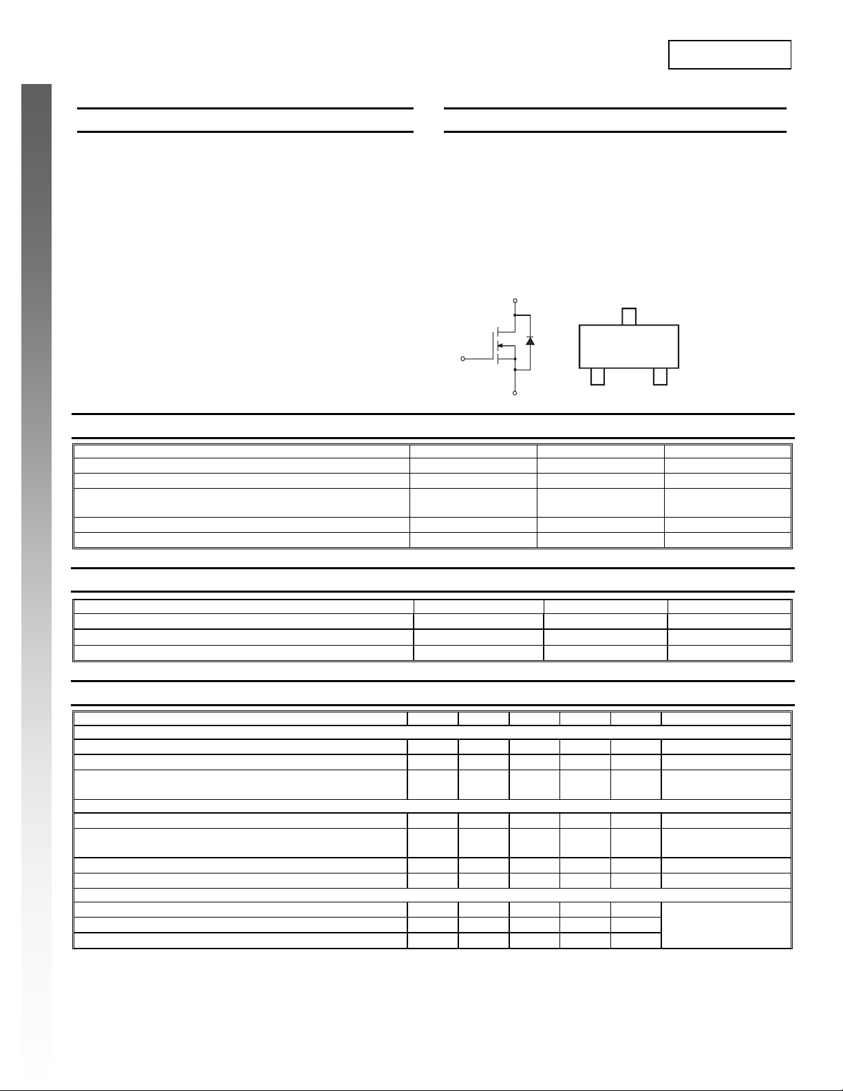
SOT-323
Gate
TOP VIEW
V
V
Drain
Source
EQUIVALENT CIRCUIT
DSS
GSS
ID
IDM
IS
D
GS
Pin Configuration
28 V
±12
1.6
1.2
6.4 A
1.5 A
V
A
Thermal Characteristics
Characteristic Symbol Value Unit
Total Power Dissipation (Note 1)
Thermal Resistance, Junction to Ambient @TA = 25°C (Note 1)
Operating and Storage Temperature Range
Electrical Characteristics @T
Characteristic Symbol Min Typ Max Unit Test Condition
OFF CHARACTERISTICS (Note 4)
Drain-Source Breakdown Voltage
Zero Gate Voltage Drain Current
Gate-Body Leakage
ON CHARACTERISTICS (Note 4)
Gate Threshold Voltage
Static Drain-Source On-Resistance
Forward Transconductance
Source-Drain Diode Forward Voltage
DYNAMIC CHARACTERISTICS
Input Capacitance
Output Capacitance
Reverse Transfer Capacitance
Notes: 1. Device mounted on 1in2 FR-4 PCB on 2oz. Copper. t ≤ 10 sec.
3. Diodes Inc.'s "Green" policy can be found on our website at http://www.diodes.com/products/lead_free/index.php.
DMN3150LW
Document number: DS31514 Rev. 1 - 2
2. No purposefully added lead.
4. Short duration pulse test used to minimize self-heating effect.
= 25°C unless otherwise specified
A
P
R
θ
T
J, TSTG
BV
DSS
I
DSS
I
GSS
V
R
DS(ON)
GS(th)
0.62 0.94 1.4 V
|Yfs|
V
SD
C
iss
C
oss
C
rss
1 of 4
www.diodes.com
D
JA
28
⎯ ⎯
⎯ ⎯
⎯ ⎯
⎯
⎯
⎯
73
115
5.4
⎯ ⎯
⎯
⎯
⎯
305
74
48
350 mW
357 °C/W
-55 to +150 °C
V
V
= 0V, ID = 250μA
800 nA
±80
±800
nA
GS
V
= 28V, VGS = 0V
DS
VGS = ±12V, VDS = 0V
VGS = ±19V, VDS = 0V
VDS = VGS, ID = 250μA
88
138
⎯
1.16 V
⎯
⎯
⎯
VGS = 4.5V, ID = 1.6A
mΩ
VGS = 2.5V, ID = 1.2A
S
VDS = 5V, ID = 2.7A
VGS = 0V, IS = 1.5A
pF
VDS = 5V, VGS = 0V
pF
f = 1.0MHz
pF
August 2008
© Diodes Incorporated
Page 2
W
R
TATIC DR
OUR
C
C, CAPACITANC
F
R
T
T
C
RAIN-SOUR
C
8
6
4
2
0
NEW PRODUCT
V , DRAIN-SOURCE VOLTAGE (V)
DS
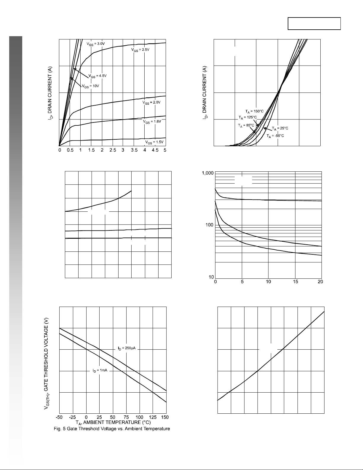
Fig. 1 Typical Output Characteristics
0.16
E
0.12
Ω
AIN-S
0.08
, S
ON-RESISTANCE ( )
0.04
DS(on)
V = 2.5V
GS
V = 4.5V
GS
V = 10V
GS
DMN3150L
8
V = 5V
DS
Pulsed
6
4
2
0
0.5 1 1.5 2 2.5 3
V , GATE-SOURCE VOLTAGE (V)
GS
Fig. 2 Typical Transfer Characteristics
f = 1 MHz
T = 25°C
A
)
E (p
C
iss
C
oss
C
rss
0
0246
I , DRAIN CURRENT (A)
D
On-Resistance
Fig. 3
vs. Drain C urrent and Gat e Volt age
1.4
1.2
1.0
0.8
8
V , DRAIN-SOURCE VOLTAGE (V)
DS
Fig. 4 Typical Total Capacitance
1.6
E
1.4
V = 4.5V
1.2
D
I
A
1.0
GS
I = 1.6A
D
, S
DS(ON)
0.6
0.4
ON-RESISTANCE (NORMALIZED)
0.8
0.6
-50 -25 0 25 50 75 100 125 150
T , AMBIENT TEMPERATURE (C)
Fig. 6 Normalized Static Drain-Source On-Resistance
A
vs. Ambien t T empe rature
DMN3150LW
Document number: DS31514 Rev. 1 - 2
2 of 4
www.diodes.com
August 2008
© Diodes Incorporated
Page 3

W
NEW PRODUCT
8
6
4
2
0
0.5 0.6 0.7 0.8 0.9 1.0 1.1 1.2
Ordering Information (Note 5)
Part Number Case Packaging
DMN3150LW-7 SOT-323 3000/Tape & Reel
Notes: 5. For packaging details, go to our website at http://www.diodes.com/datasheets/ap02007.pdf.
Marking Information
Date Code Key
Year 2008 2009 2010 2011 2012 2013 2014 2015
Code V W X Y Z A B C
Month Jan Feb Mar Apr May Jun Jul Aug Sep Oct Nov Dec
Code 1 2 3 4 5 6 7 8 9 O N D
31N
31N = Product Type Marking Code
YM = Date Code Marking
Y = Year (ex: V = 2008)
YM
M = Month (ex: 9 = September)
Package Outline Dimensions
DMN3150LW
Document number: DS31514 Rev. 1 - 2
K
J
A
TOP VIEW
G
H
DF
C
B
M
L
3 of 4
www.diodes.com
Dim Min Max Typ
SOT-323
A 0.25 0.40 0.30
B 1.15 1.35 1.30
C 2.00 2.20 2.10
D - - 0.65
F 0.30 0.40 0.425
G 1.20 1.40 1.30
H 1.80 2.20 2.15
J 0.0 0.10 0.05
K 0.90 1.00 1.00
L 0.25 0.40 0.30
M 0.10 0.18 0.11
0° 8° -
α
All Dimensions in mm
DMN3150L
August 2008
© Diodes Incorporated
Page 4

W
DMN3150L
Suggested Pad Layout
Diodes Incorporated and its subsidiaries reserve the right to make modifications, enhancements, improvements, corrections or other changes
NEW PRODUCT
without further notice to any product herein. Diodes Incorporated does not assume any liability arising out of the application or use of any product
described herein; neither does it convey any license under its patent rights, nor the rights of others. The user of products in such applications shall
assume all risks of such use and will agree to hold Diodes Incorporated and all the companies whose products are represented on our website,
harmless against all damages.
Diodes Incorporated products are not authorized for use as critical components in life support devices or systems without the expressed written
approval of the President of Diodes Incorporated.
Y
Z
C
Dimensions Value (in mm)
Z 2.8
X 0.7
Y 0.9
C 1.9
E 1.0
X E
IMPORTANT NOTICE
LIFE SUPPORT
DMN3150LW
Document number: DS31514 Rev. 1 - 2
4 of 4
www.diodes.com
August 2008
© Diodes Incorporated
 Loading...