

Diodes DMN2990UFA User Manual

NEW PRODUCT
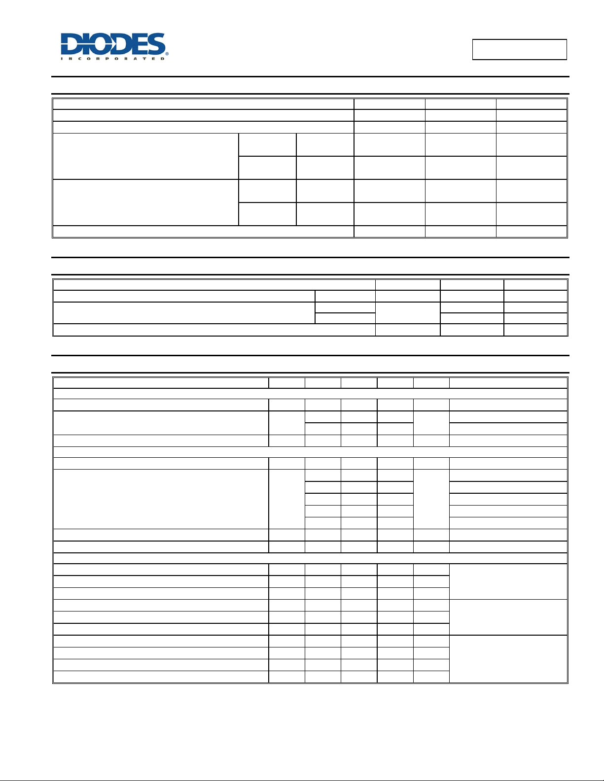
Product Summary
I
max
D
V
R
(BR)DSS
0.99 @ V
20V
1.2 @ VGS = 2.5V
1.8 @ VGS = 1.8V
2.4 @ VGS = 1.5V
DS(ON)
max
= 4.5V
GS
TA = +25°C
510mA
470mA
380mA
330mA
Description
This MOSFET has been designed to minimize the on-state resistance
(R
) and yet maintain superior switching performance, making it
DS(on)
ideal for high efficiency power management applications.
Applications
General Purpose Interfacing Switch
Power Management Functions
Analog Switch
ESD PROTECTED
Bottom View
Ordering Information (Note 4)
DMN2990UFA
20V N-CHANNEL ENHANCEMENT MODE MOSFET
Features and Benefits
Low Package Profile, 0.4mm Maximum Package height
0.48mm
Low On-Resistance
Very low Gate Threshold Voltage, 1.0V max
ESD Protected Gate
Totally Lead-Free & Fully RoHS Compliant (Notes 1 & 2)
Halogen and Antimony Free. “Green” Device (Note 3)
Qualified to AEC-Q101 standards for High Reliability
2
package footprint, 16 times smaller than SOT23
Mechanical Data
Case: X2-DFN0806-3
Case Material: Molded Plastic, “Green” Molding Compound.
UL Flammability Classification Rating 94V-0
Moisture Sensitivity: Level 1 per J-STD-020
Terminals: Finish – NiPdAu over Copper leadframe.
Drain
e4
Source
Body
Diode
Solderable per MIL-STD-202, Method 208
Weight: 0.001 grams (approximate)
Gate
S
D
G
Top View
Package Pin Configuration
Gate
Protection
Diode
Equivalent Circuit
Part Number Case Packaging
DMN2990UFA-7B X2-DFN0806-3 10K/Tape & Reel
Notes: 1. No purposely added lead. Fully EU Directive 2002/95/EC (RoHS) & 2011/65/EU (RoHS 2) compliant.
2. See http://www.diodes.com/quality/lead_free.html for more information about Diodes Incorporated’s definitions of Halogen- and Antimony-free, "Green"
and Lead-free.
3. Halogen- and Antimony-free "Green” products are defined as those which contain <900ppm bromine, <900ppm chlorine (<1500ppm total Br + Cl) and
<1000ppm antimony compounds.
4. For packaging details, go to our website at http://www.diodes.com/products/packages.html.
Marking Information
DMN2990UFA
Document number: DS35765 Rev. 3 - 2
DMN2990UFA-7B
NW
Top View
Bar Denotes Gate
and Source Side
www.diodes.com
NW = Product Type Marking Code
1 of 6
June 2013
© Diodes Incorporated
V
V
DMN2990UFA
Maximum Ratings (@T
Drain-Source Voltage
Gate-Source Voltage
Continuous Drain Current (Note 5) VGS = 4.5V
Continuous Drain Current (Note 5) VGS = 1.8V
Pulsed Drain Current (Note 6)
= +25°C, unless otherwise specified.)
A
Characteristic Symbol
V
DSS
V
GSS
= +25°C
Steady
State
t<10s
Steady
State
t<10s
T
A
T
= +70°C
A
= +25°C
T
A
T
= +70°C
A
= +25°C
T
A
T
= 70°C
A
T
= +25°C
A
= +70°C
T
A
I
I
I
I
I
DM
alue Units
D
D
D
D
20 V
±8 V
510
410
610
490
380
300
450
360
mA
mA
mA
mA
800 mA
NEW PRODUCT
Thermal Characteristics (@T
= +25°C, unless otherwise specified.)
A
Characteristic Symbol
Total Power Dissipation (Note 5) Steady state
Thermal Resistance, Junction to Ambient (Note 5)
Steady state
t<10s 220 °C/W
Operating and Storage Temperature Range
P
R
T
J, TSTG
alue Units
D
JA
400 mW
310 °C/W
-55 to +150 °C
Electrical Characteristics (@T
= +25°C, unless otherwise specified.)
A
Characteristic Symbol Min Typ Max Unit Test Condition
OFF CHARACTERISTICS (Note 7)
Drain-Source Breakdown Voltage
Zero Gate Voltage Drain Current @TC = +25°C I
Gate-Source Leakage
BV
I
DSS
DSS
GSS
20
— —
— —
— —
—
— V
100
50
nA
±100 nA
VGS = 0V, ID = 250A
V
= 16V, VGS = 0V
DS
= 5V, VGS = 0V
V
DS
VGS = ±5V, VDS = 0V
ON CHARACTERISTICS (Note 7)
Gate Threshold Voltage
Static Drain-Source On-Resistance
Forward Transfer Admittance
Diode Forward Voltage
V
R
DS(ON)
|Y
V
GS(th)
fs
SD
0.4 — 1.0 V
—
—
—
—
—
180
|
- 0.6 1.0 V
0.60 0.99
0.75 1.2
0.90 1.8
1.2 2.4
2.0 —
— —
VDS = VGS, ID = 250A
= 4.5V, ID = 100mA
V
GS
= 2.5V, ID = 50mA
V
GS
Ω
mS
= 1.8V, ID = 20mA
V
GS
= 1.5V, ID = 10mA
V
GS
= 1.2V, ID = 1mA
V
GS
VDS = 10V, ID = 400mA
VGS = 0V, IS = 150mA
DYNAMIC CHARACTERISTICS (Note 8)
Input Capacitance
Output Capacitance
Reverse Transfer Capacitance
Total Gate Charge
Gate-Source Charge
Gate-Drain Charge
Turn-On Delay Time
Turn-On Rise Time
Turn-Off Delay Time
Turn-Off Fall Time
Notes: 5. Device mounted on FR-4 PCB, with minimum recommended pad layout.
6. Device mounted on minimum recommended pad layout test board, 10s pulse duty cycle = 1%.
7. Short duration pulse test used to minimize self-heating effect.
8. Guaranteed by design. Not subject to product testing.
C
C
C
Q
Q
Q
t
D(on)
t
D(off)
iss
oss
rss
gd
t
t
g
gs
r
f
— 27.6 55.2 pF
—
—
—
—
—
—
—
—
—
4.0 8.0 pF
2.8 5.6 pF
0.5
0.07
0.07
4.0
3.3
19.0
6.4
—
—
—
—
—
—
—
nC
nC
nC
ns
ns
ns
ns
V
= 16V, VGS = 0V,
DS
f = 1.0MHz
V
= 4.5V, VDS = 10V,
GS
= 250mA
I
D
V
= 10V, VGS = 4.5V,
DD
R
= 47, RG = 10,
L
I
= 200mA
D
DMN2990UFA
Document number: DS35765 Rev. 3 - 2
2 of 6
www.diodes.com
June 2013
© Diodes Incorporated
 Loading...