Diodes DMN26D0UT User Manual

θ
n
Please click here to visit our online spice models database.
Features
• Low On-Resistance:
• 3.0 Ω @ 4.5V
• 4.0 Ω @ 2.5V
• 6.0 Ω @ 1.8V
• 10 Ω @ 1.5V
• Very Low Gate Threshold Voltage, 1.0V max
• Low Input Capacitance
• Fast Switching Speed
• Low Input/Output Leakage
• Ultra-Small Surface Mount Package
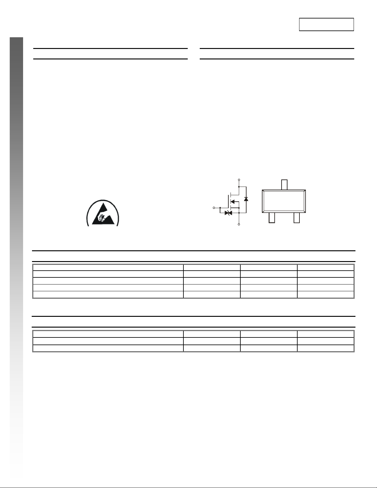
• ESD Protected Gate
• Lead, Halogen, and Antimony Free By Design/RoHS
Compliant (Note 2)
• "Green" Device (Note 3)
• Qualified to AEC-Q101 Standards for High Reliability
NEW PRODUCT
Maximum Ratings @T
Drain Source Voltage
Gate-Source Voltage
Drain Current (Note 1)
Pulsed Drain Current TP = 10µs IDM
ESD PROTECTED
= 25°C unless otherwise specified
A
TOP VIEW
Characteristic Symbol Value Unit
DMN26D0UT
N-CHANNEL ENHANCEMENT MODE MOSFET
Mechanical Data
• Case: SOT-523
• Case Material: Molded Plastic, “Green” Molding Compound. UL
Flammability Classification Rating 94V-0
• Moisture Sensitivity: Level 1 per J-STD-020
• Terminal Connections: See Diagram
• Terminals: Finish – Matte Tin annealed over Alloy 42 leadframe.
Solderable per MIL-STD-202, Method 208
• Marking Information: See Page 4
• Ordering Information: See Page 4
• Weight: 0.002 grams (approximate)
Drai
D
Gate
Gate
Protection
Diode
EQUIVALENT CIRCUIT
V
DSS
V
GSS
I
D
Source
G
TOP VIEW
20 V
±10
230 mA
805 mA
S
V
Thermal Characteristics @T
= 25°C unless otherwise specified
A
Total Power Dissipation (Note 1)
Thermal Resistance, Junction to Ambient (Note 1)
Operating and Storage Temperature Range
Notes: 1. Device mounted on FR-4 PCB, 1 inch x 0.85 inch x 0.062 inch; pad layout as shown on Diodes Inc. suggested pad layout document AP02001, which
can be found on our website at http://www.diodes.com/datasheets/ap02001.pdf.
2. No purposefully added lead.
3. Diodes Inc.’s “Green” policy can be found on our website at http://www.diodes.com/products/lead_free/index.php.
DMN26D0UT
Document number: DS31854 Rev. 2 - 2
P
D
R
JA
T
, T
J
1 of 6
www.diodes.com
STG
300 mW
417
-55 to +150
°C/W
°C
September 2009
© Diodes Incorporated

)
)
r
)
R
C
U
R
R
T
R
CUR
RENT
Electrical Characteristics @T
= 25°C unless otherwise specified
A
Characteristic Symbol Min Typ Max Unit Test Condition
OFF CHARACTERISTICS (Note 4)
Drain-Source Breakdown Voltage
Zero Gate Voltage Drain Current @ TC = 25°C I
Gate-Body Leakage
ON CHARACTERISTICS (Note 4)
Gate Threshold Voltage
Static Drain-Source On-Resistance
Forward Transconductance
Source-Drain Diode Forward Voltage
DYNAMIC CHARACTERISTICS
Input Capacitance
NEW PRODUCT
Output Capacitance
Reverse Transfer Capacitance
SWITCHING CHARACTERISTICS, VGS = 4.5V (Note 5)
Turn-On Delay Time
Rise Time
Turn-Off Delay Time
Fall Time
Notes: 4. Short duration pulse test used to minimize self-heating effect.
5. Switching characteristics are independent of operating junction temperature.
0.8
0.7
V = 8V
GS
V = 4.5V
GS
BV
DSS
DSS
I
GSS
V
GS(th
R
DS (ON)
|Y
fs
V
SD
C
iss
C
oss
C
rss
t
d(on
t
⎯
t
d(off
t
⎯
f
|
⎯
⎯
⎯
⎯
20
⎯ ⎯
⎯ ⎯
0.5
⎯
⎯
⎯
⎯
⎯
⎯
1.8
2.4
2.9
3.7
5.4
242
0.5
14.1
⎯
2.9
1.6
13.4
15.2
0.4
⎯ ⎯
500 nA
±1
±500
±100
⎯
1.0 V
3.0
4.0
6.0
10.0
15.0
⎯
⎯
1.0 V
⎯
⎯
⎯
3.8
7.9
⎯
⎯
⎯
⎯
V = 10V
DS
DMN26D0UT
V
V
= 0V, ID = 100μA
GS
V
= 20V, VGS = 0V
DS
V
= ±10V, VDS = 0V
μA
nA
nA
mS
pF
pF
pF
GS
= ±8V, VDS = 0V
V
GS
V
= ±5V, VDS = 0V
GS
VDS = VGS, ID = 250μA
V
= 4.5V, ID = 100mA
GS
= 2.5V, ID = 50mA
V
GS
Ω
V
= 1.8V, ID = 20mA
GS
= 1.5V, ID = 10mA
V
GS
V
= 1.2V, ID = 1mA
GS
VDS =10V, ID = 0.1A
VGS = 0V, IS = 115mA
V
= 15V, VGS = 0V
DS
f = 1.0MHz
= 4.5V, VDD = 10V
V
GS
ns
= 200mA, RG = 2.0Ω
I
D
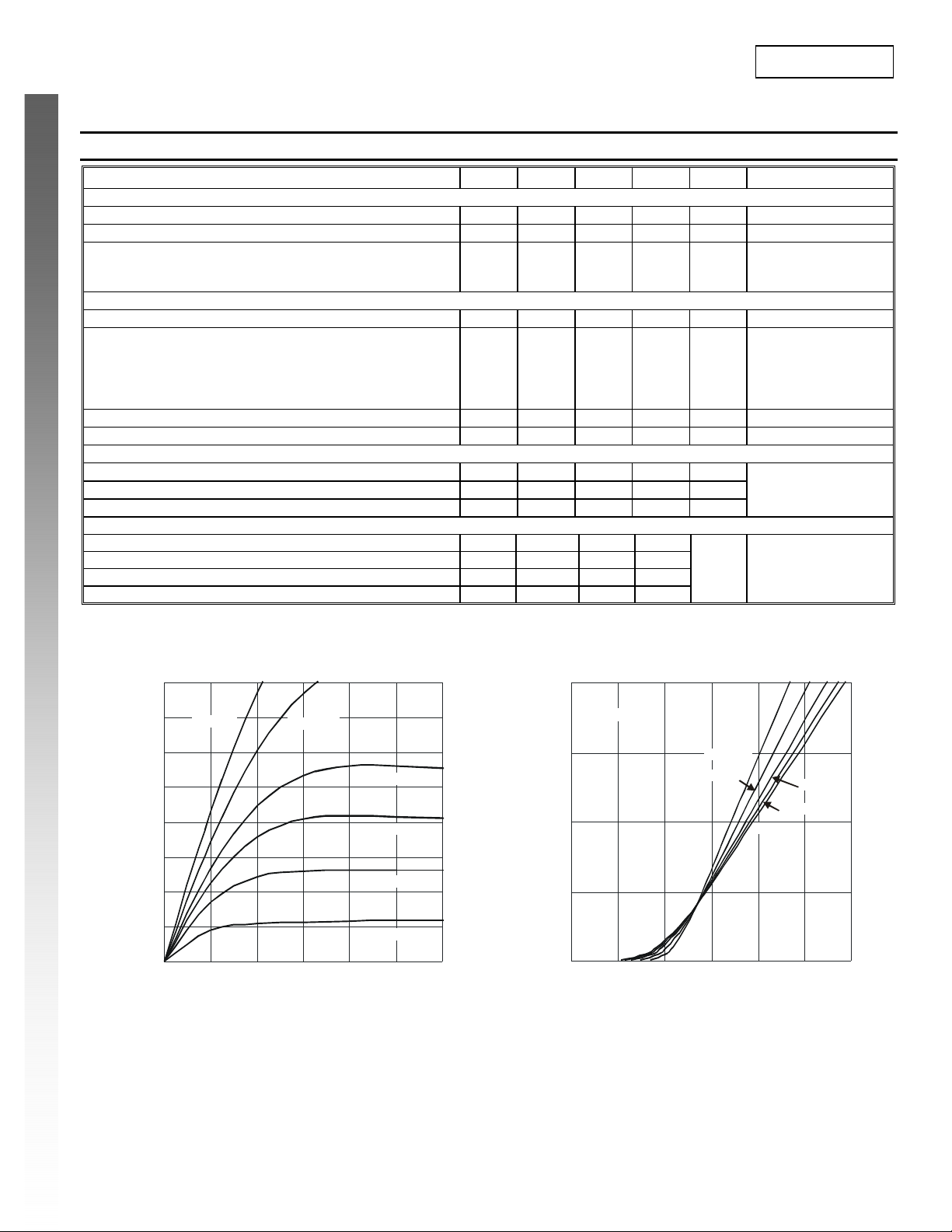
0.6
(A)
0.5
EN
0.4
AIN
0.3
D
I, D
0.2
0.1
0
0 0.5 1 1.5 2 2.5 3
V , DRAIN-SOURCE VOLTAGE (V)
DS
V = 3.0V
GS
V = 2.5V
GS
V = 2.0V
GS
V = 1.5V
GS
Fig. 1 Typica l O ut put Chara cteristic
0.3
(A)
0.2
AIN
D
I, D
0.1
0
0 0.5 1 1.5 2 2.5 3
V , GATE-SOURCE VOLTAGE (V)
GS
Fig. 2 Typical Transfer Characteristic
T = -55°C
A
T = 25°C
A
T = 125°C
A
T = 150°C
A
T = 85°C
A
DMN26D0UT
Document number: DS31854 Rev. 2 - 2
2 of 6
www.diodes.com
September 2009
© Diodes Incorporated
 Loading...