Diodes DMN2600UFB User Manual

q
Features
• Low On-Resistance
• Low Gate Threshold Voltage
• Fast Switching Speed
• Ultra-Small Surface Mount Package
• Lead Free By Design/RoHS Compliant (Note 1)
• "Green" Device (Note 2)
• ESD Protected Gate 1kV
• Qualified to AEC-Q101 Standards for High Reliability
NEW PRODUCT
ESD PROTECTED TO 1kV
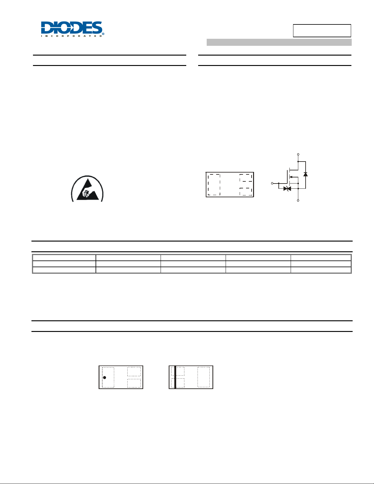
Bottom View
DFN1006-3
DMN2600UFB
25V N-CHANNEL ENHANCEMENT MODE MOSFET
Mechanical Data
• Case: DFN1006-3
• Case Material: Molded Plastic, “Green” Molding Compound.
UL Flammability Classification Rating 94V-0
• Moisture Sensitivity: Level 1 per J-STD-020
• Terminals: Finish – NiPdAu over Copper leadframe. Solderable
per MIL-STD-202, Method 208
• Weight: 0.001 grams (approximate)
Drain
Body
Diode
Source
D
Top View
Internal Schematic
S
G
Gate
Gate
Protection
Diode
E
uivalent Circuit
Ordering Information (Note 3)
Part Number Marking Reel size (inches) Tape width (mm) Quantity per reel
DMN2600UFB-7 NA 7 8 3000
DMN2600UFB-7B
Notes: 1. No purposefully added lead
2. Diodes Inc's "Green" policy can be found on our website at http://www.diodes.com.
3. For packaging details, go to our website at http://www.diodes.com.
NA
7 8 10,000
Marking Information
DMN2600UFB
Document number: DS31983 Rev. 4 - 2
DMN2600UFB-7 DMN2600UFB-7B
NANA
Top View
Dot Denotes
Drain Side
Top View
Bar Denotes Gate
and Source Side
1 of 6
www.diodes.com
NA = Product Type Marking Code
March 2011
© Diodes Incorporated

)
g
g
g
g
r
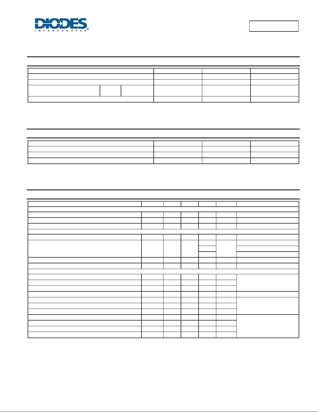
Maximum Ratings @T
Characteristic Symbol Value Unit
Drain-Source Voltage
Gate-Source Voltage
Continuous Drain Current (Note 4)
Pulsed Drain Current
Thermal Characteristics @T
Characteristic Symbol Value Unit
Power Dissipation (Note 4)
Thermal Resistance, Junction to Ambient @T
NEW PRODUCT
Operating and Storage Temperature Range
= 25°C unless otherwise specified
A
T
Steady
State
= 25°C unless otherwise specified
A
= 25°C R
A
= 25°C
A
T
= 85°C
A
T
V
V
J
DSS
GSS
I
I
DM
P
, T
D
D
θJA
STG
DMN2600UFB
25 V
±8 V
1.3
0.9
A
3.0 A
0.54 W
234 °C/W
-55 to +150 °C
Electrical Characteristics @T
= 25°C unless otherwise specified
A
Characteristic Symbol Min Typ Max Unit Test Condition
OFF CHARACTERISTICS (Note 5)
Drain-Source Breakdown Voltage
Zero Gate Voltage Drain Current TJ = 25°C I
Gate-Source Leakage
BV
DSS
I
GSS
DSS
25 - - V
- - 1
- - 10
VGS = 0V, ID = 250μA
μA
μA
= 25V, VGS = 0V
V
DS
= ±8V, VDS = 0V
V
GS
ON CHARACTERISTICS (Note 5)
Gate Threshold Voltage
Static Drain-Source On-Resistance
Forward Transfer Admittance
Diode Forward Voltage
V
GS(th
R
DS (ON)
|Y
V
fs
SD
0.45 - 1.0 V
350
- -
450
600
40 - - mS
|
- - 1.2 V
VDS = VGS, ID = 250μA
V
= 4.5V, ID = 200mA
mΩ
GS
V
= 2.5V, ID = 100mA
GS
V
= 1.8V, ID = 75mA
GS
VDS = 3V, ID = 200mA
VGS = 0V, IS = 300mA
DYNAMIC CHARACTERISTICS (Note 6)
Input Capacitance
Output Capacitance
Reverse Transfer Capacitance
Gate Resistance
Total Gate Charge
Gate-Source Charge
Gate-Drain Charge
Turn-On Delay Time
Turn-On Rise Time
Turn-Off Delay Time
Turn-Off Fall Time
Notes: 4. Device mounted on FR-4 substrate PCB board, with minimum recommended pad layout.
5. Short duration pulse test used to minimize self-heating effect.
6. Guaranteed by design. Not subject to production testing.
C
C
C
R
Q
Q
Q
t
D(on)
t
D(off)
iss
oss
rss
t
t
s
d
f
- 70.13 -
- 7.56 -
- 5.59 -
- 72.3 -
- 0.85 -
- 0.16 -
- 0.11 -
- 4.1 -
- 11.5 -
- 34.8 -
- 20.9 -
pF
pF
pF
Ω
nC
nC
nC
= 15V, VGS = 0V,
V
DS
f = 1.0MHz
VDS =0V, VGS = 0V, f = 1MHz
= 4.5V, VDS = 15V,
V
GS
= 1A
I
D
ns
ns
ns
= 15V, RL=15Ω
V
DS
V
= 10V, RG = 6Ω
GS
ns
DMN2600UFB
Document number: DS31983 Rev. 4 - 2
2 of 6
www.diodes.com
March 2011
© Diodes Incorporated
 Loading...