Diodes DMN2300UFB4 User Manual

A
f
Product Line o
Diodes Incorporated
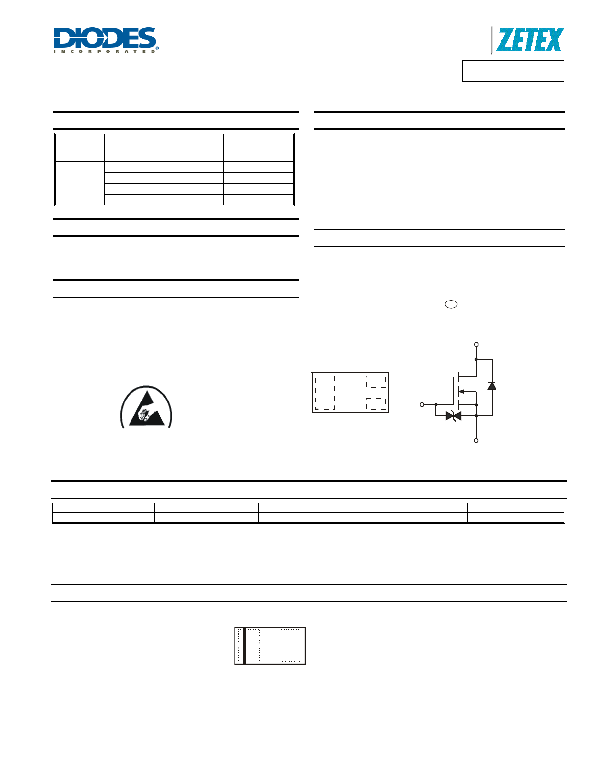
Product Summary
I
V
R
(BR)DSS
175mΩ @ V
20V
240mΩ @ VGS = 2.5V
360mΩ @ VGS = 1.8V
500mΩ @ VGS = 1.5V
DS(ON)
= 4.5V
GS
D
TA = +25°C
(Note 5)
1.30A
1.11A
0.91A
0.82A
Description
This MOSFET has been designed to minimize the on-state resistance
(R
) and yet maintain superior switching performance, making it
DS(on)
ideal for high efficiency power management applications.
Applications
• Load switch
ESD PROTECTED TO 2kV
X2-DFN1006-3
Bottom View
DMN2300UFB4
20V N-CHANNEL ENHANCEMENT MODE MOSFET
Features
• Footprint of just 0.6mm2 – thirteen times smaller than SOT23
• 0.4mm profile – ideal for low profile applications
• Low Gate Threshold Voltage
• Fast Switching Speed
• ESD Protected Gate 2KV
• Totally Lead-Free & Fully RoHS Compliant (Notes 1 & 2)
• Halogen and Antimony Free. “Green” Device (Note 3)
• Qualified to AEC-Q101 Standards for High Reliability
Mechanical Data
• Case: X2-DFN1006-3
• Case Material: Molded Plastic, “Green” Molding Compound. UL
Flammability Classification Rating 94V-0
• Moisture Sensitivity: Level 1 per J-STD-020
• Terminals: Finish – NiPdAu over Copper leadframe. Solderable
per MIL-STD-202, Method 208
• Weight: 0.001 grams (approximate)
S
D
G
Top View
Internal Schematic
Gate
e4
Gate
Protection
Diode
Equivalent Circuit
Drain
Source
Body
Diode
Ordering Information (Note 4)
Part Number Marking Reel size (inches) Tape width (mm) Quantity per reel
DMN2300UFB4-7B NL 7 8 10,000
Notes: 1. No purposely added lead. Fully EU Directive 2002/95/EC (RoHS) & 2011/65/EU (RoHS 2) compliant.
2. See http://www.diodes.com for more information about Diodes Incorporated’s definitions of Halogen- and Antimony-free, "Green " and Lead-free.
4. For packaging details, go to our website at http://www.diodes.com.
3. Halogen- and Antimony-free "Green” products are defined as those which contain <900ppm bromine, <900ppm chlorine (<1500ppm total Br + Cl) and
<1000ppm antimony compounds.
Marking Information
DMN2300UFB4-7B
DMN2300UFB4
Document number: DS35269 Rev. 4 - 2
NL
Top View
Bar Denotes Gate
and Source Side
www.diodes.com
NL = Product Type Marking Code
1 of 7
September 2012
© Diodes Incorporated

A
f
)
g
g
g
g
)
r
)
Product Line o
Diodes Incorporated
DMN2300UFB4
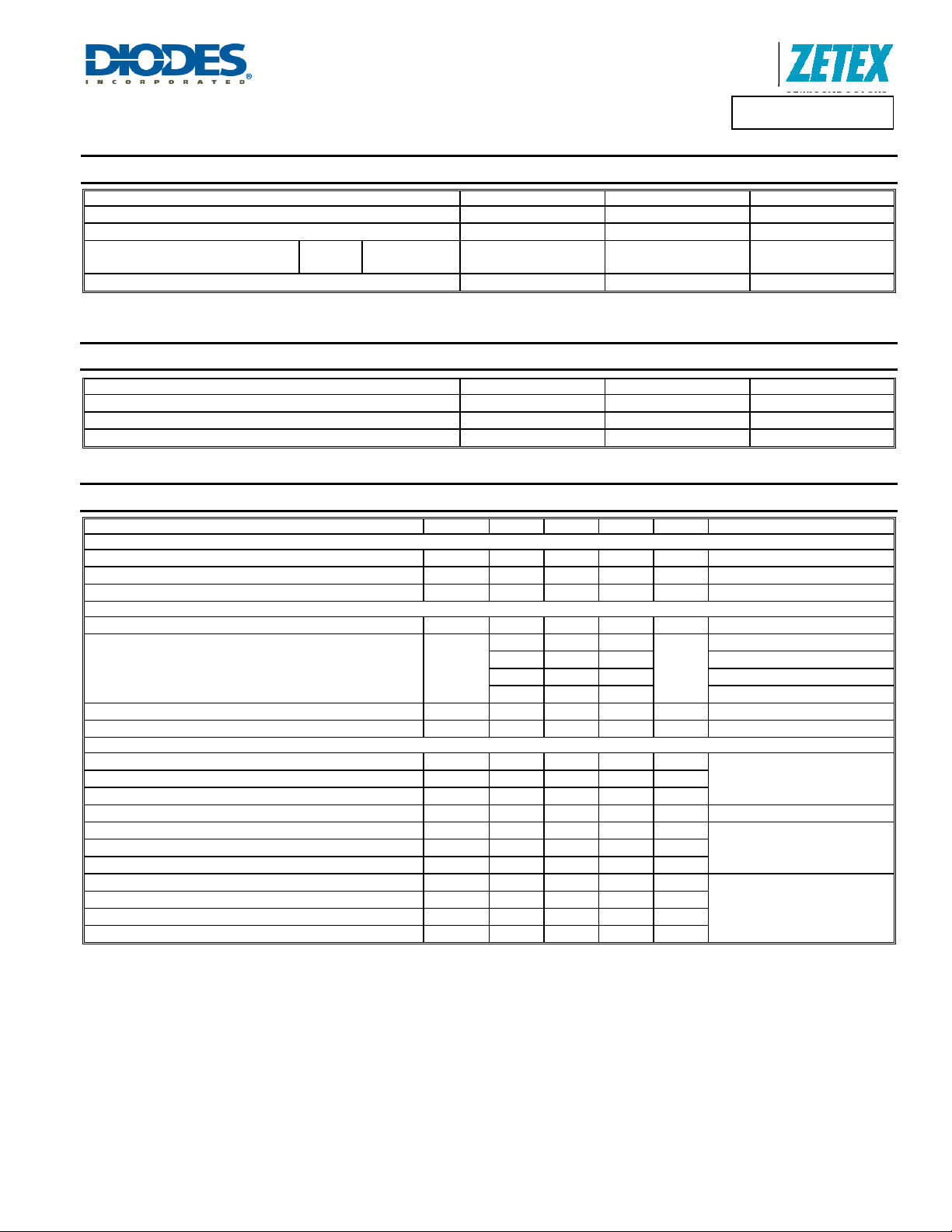
Maximum Ratings (@T
= +25°C, unless otherwise specified.)
A
Characteristic Symbol Value Unit
Drain-Source Voltage
Gate-Source Voltage
Continuous Drain Current (Note 5)
Pulsed Drain Current (Note 6)
Steady
State
T
= +25°C
A
= +85°C
T
A
V
V
DSS
GSS
I
I
DM
D
20 V
±8 V
1.30
0.96
A
6 A
Thermal Characteristics
Characteristic Symbol Value Unit
Power Dissipation (Note 5)
Thermal Resistance, Junction to Ambient @TA = +25°C R
Operating and Storage Temperature Range
P
D
θJA
T
, T
J
STG
Electrical Characteristics (@T
= +25°C, unless otherwise specified.)
A
Characteristic Symbol Min Typ Max Unit Test Condition
OFF CHARACTERISTICS (Note 7)
Drain-Source Breakdown Voltage
Zero Gate Voltage Drain Current TJ = +25°C I
Gate-Source Leakage
BV
I
DSS
DSS
GSS
20 — — V
— — 1 µA
— — 10 µA
ON CHARACTERISTICS (Note 7)
Gate Threshold Voltage
V
GS(th
0.45 — 0.95 V
— — 175
Static Drain-Source On-Resistance
R
DS (ON)
— — 240
— — 360
— — 500
Forward Transfer Admittance
Diode Forward Voltage
|
|Y
fs
V
SD
40 — — mS
— 0.7 1.2 V
DYNAMIC CHARACTERISTICS
Input Capacitance
Output Capacitance
Reverse Transfer Capacitance
Gate Resistance
Total Gate Charge
Gate-Source Charge
Gate-Drain Charge
Turn-On Delay Time
Turn-On Rise Time
Turn-Off Delay Time
Turn-Off Fall Time
Notes: 5. Device mounted on FR-4 PCB, with minimum recommended pad layout.
6. Device mounted on minimum recommended pad layout test board, 10µs pulse duty cycle = 1%.
7. Short duration pulse test used to minimize self-heating effect.
DMN2300UFB4
Document number: DS35269 Rev. 4 - 2
C
iss
C
oss
C
rss
R
Q
Q
s
Q
d
t
D(on
t
t
D(off
t
f
www.diodes.com
— 64.3 — pF
— 6.1 — pF
— 4.5 — pF
— 70 — Ω
— 1.6 — nC
— 0.2 — nC
— 0.2 — nC
— 3.5 — ns
— 2.8 — ns
— 38 — ns
— 13 — ns
2 of 7
500 mW
250 °C/W
-55 to +150 °C
VGS = 0V, ID = 10µA
VDS = 20V, VGS = 0V
VGS = ±8V, VDS = 0V
VDS = VGS, ID = 250μA
V
= 4.5V, ID = 1A
GS
= 2.5V, ID = 750mA
V
mΩ
GS
= 1.8V, ID = 500mA
V
GS
= 1.5V, ID = 200mA
V
GS
VDS = 3V, ID = 30mA
VGS = 0V, IS = 300mA
V
= 25V, VGS = 0V,
DS
f = 1.0MHz
VDS = 0V, VGS = 0V, f = 1MHz
V
= 4.5V, VDS = 15V,
GS
= 1A
I
D
V
= 10V, ID = 1A
DS
V
= 10V, RG = 6Ω
GS
September 2012
© Diodes Incorporated

A
f
R
CUR
RENT
R
CUR
RENT
R
RAIN-SOUR
CE O
N-R
TAN
C
R
R
OUR
CE ON-R
TANC
R
RAIN
OUR
CE O
N
R
T
N
C
Product Line o
Diodes Incorporated
DMN2300UFB4
2.0
1.5
(A)
V = 4.5V
GS
V = 2.5V
GS
V = 2.0V
GS
V = 1.8V
GS
V = 1.5V
GS
1.0
AIN
D
I, D
0.5
V = 1.2V
GS
0
012 345
V , DRAIN-SOURCE VOLTAGE (V)
DS
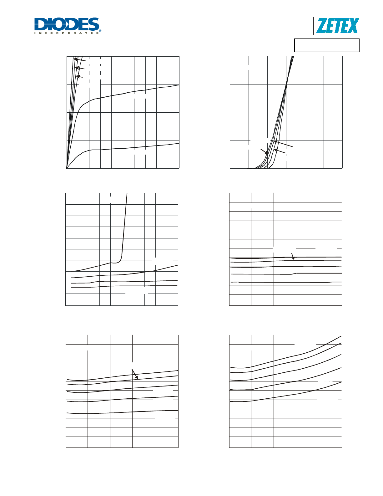
Figure 1 Typical Output C haracterist ic
1.0
Ω
V = 1.5V
GS
0.8
2.0
V = 5V
DS
1.5
(A)
1.0
AIN
D
I, D
0.5
0
0 0.5 1.0 1.5 2.0 2.5 3.0
0.6
Ω
E ( )
0.5
T = 150°C
A
T = 125°C
A
V , GATE-SOURCE VOLTAGE (V)
GS
Figure 2 Typical Transfer Characteristic
V = 4.5V
GS
T = 25°C
A
T = -55°C
A
T = 85°C
A
0.6
0.4
0.2
V = 4.5V
GS
DS(ON)
R , DRAIN-SOURCE ON-RESISTANCE ( )
0
0 0.4 0.8 1.2 1.6 2.0
I , DRAIN-SOURCE CURRENT (A)
D
Figure 3 Typical On-Resistance
vs. Drain C urrent an d G at e Vol t age
0.6
Ω
V = 1.8V
E ( )
ESIS
0.5
0.4
GS
T = 125°C
A
T = 150°C
0.3
0.2
AIN-S
0.1
, D
V = 1.8V
GS
V = 2.5V
GS
A
T = 85°C
A
T = 25°C
A
T = -55°C
A
0.4
ESIS
0.3
T = 125°C
A
0.2
T = 25°C
A
0.1
, D
DS(ON)
0
0 0.2 0.4 0.6 0.8 1.0
I , DRAIN CURRENT (A)
D
Figure 4 Typical On-Resistance
vs. Drain C urrent an d Temperature
0.6
Ω
V = 1.5V
E ( )
0.5
GS
T = 150°C
A
A
8
=
0.4
ESIS
T
A
-
0.3
0.2
-S
0.1
, D
T = 150°C
A
T = 85°C
A
T = -55°C
A
5
2
1
=
T
A
C
°
5
°
5
2
=
T
A
T = -55°C
A
C
°
C
DS(ON)
0
0 0.2 0.4 0.6 0.8 1.0
I , DRAIN CURRENT (A)
D
Figure 5 Typical On-Resistance
vs. Drain C urrent an d Temperature
DMN2300UFB4
Document number: DS35269 Rev. 4 - 2
3 of 7
www.diodes.com
DS(ON)
0
0 0.2 0.4 0.6 0.8 1.0
I , DRAIN CURRENT (A)
D
Figure 6 Typical On-Resistance
vs. Drain C urrent an d Temperature
September 2012
© Diodes Incorporated
 Loading...