Diodes DDTC113TLP User Manual

y
PRE-BIASED SMALL SIGNAL SURFACE MOUNT NPN TRANSISTOR
Features
• Epitaxial Planar Die Construction
• Ultra-Small Leadless Surface Mount Package
• Ideally Suited for Automated Assembly Processes
• “Lead Free”, RoHS Compliant (Note 1)
• Halogen and Antimony Free "Green" Device (Note 2)
• Qualified to AEC-Q101 Standards for High Reliability
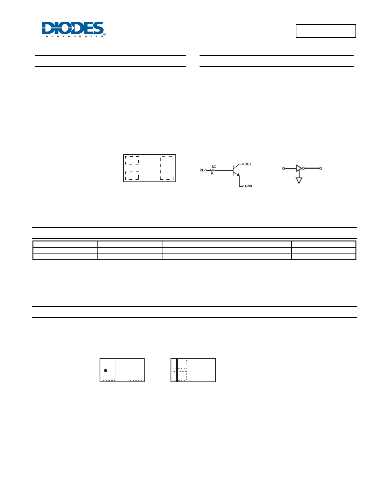
DFN1006-3
Bottom View
B
E
Top View
Pin-Out
DDTC113TLP
Mechanical Data
• Case: DFN1006-3
• Case Material: Molded Plastic. "Green” Molding Compound.
UL Flammability Classification Rating 94V-0
• Moisture Sensitivity: Level 1 per J-STD-020
• Terminals: Finish - NiPdAu over Copper leadframe. Solderable
per MIL-STD-202, Method 208
• Weight: 0.0009 grams (approximate)
C
C
1
1
10 KÙ
Device S
B
3
E
2
mbol
B
IN
1
Equivalent Inverter
E
2
Circuit
C
GND
3
OUT
Ordering Information (Note 3)
Product Marking Reel size (inches) Tape width (mm) Quantity per reel
DDTC113TLP-7 N4 7 8 3,000
DDTC113TLP-7B N4 7 8 10,000
Notes: 1. No purposefully added lead.
2. Diodes Inc's "Green" policy can be found on our website at http://www.diodes.com.
3. For packaging details, go to our website at http://www.diodes.com.
Marking Information
DDTC113TLP-7 DDTC113TLP-7B
N4N4
Top View
Dot Denotes
Collector Side
Top View
Bar Denotes Base
and Emitter Side
N4 = Product Type Marking Code
DDTC113TLP
Document number: DS30843 Rev. 8 - 2
1 of 4
www.diodes.com
February 2011
© Diodes Incorporated

)
r
)
Ω
Maximum Ratings @T
= 25°C unless otherwise specified
A
Characteristic Symbol Value Unit
Supply Voltage
Input Voltage
Output Current (IO) I
V
CC
V
IN
C(MAX
Thermal Characteristics @T
= 25°C unless otherwise specified
A
Characteristic Symbol Value Unit
Power Dissipation (Note 4)
Power Derating above 25°C
Thermal Resistance, Junction to Ambient Air (Note 4)
(Equivalent to one heated junction of NPN)
Operating and Storage Temperature Range
P
P
R
T
J, TSTG
D
de
JA
θ
Electrical Characteristics @T
= 25°C unless otherwise specified
A
Characteristic Symbol Min Typ Max Unit Test Condition
OFF CHARACTERISTICS (Note 5)
Collector-Base Breakdown Voltage
Collector-Emitter Breakdown Voltage
Emitter-Base Breakdown Voltage
Collector-Base Cutoff Current
Emitter-Base Cutoff Current
BV
BV
BV
I
CBO
I
EBO
CBO
CEO
EBO
50
50
5
⎯ ⎯
⎯ ⎯
⎯ ⎯
⎯ ⎯
⎯ ⎯
0.5
0.5
ON CHARACTERISTICS (Note 5)
DC Current Gain
Collector-Emitter Saturation Voltage
V
CE(sat
h
FE
100 380 600
⎯ ⎯
0.25 V
Input Resistance R1 0.7 1 1.3
SMALL SIGNAL CHARACTERISTICS
Current Gain-Bandwidth Product
Notes: 4. Device mounted on FR-4 PCB, 1 inch x 0.85 inch x 0.062 inch
5. Short duration pulse test used to minimize self-heating effect.
f
T
⎯
250
800
⎯
DDTC113TLP
50 V
-5 to +10 V
100 mA
250 mW
2
500 °C/W
-55 to +150 °C
V
IC = 10μA, IE = 0
V
IC = 1.0mA, IB = 0
V
IE = 50μA, IC = 0
μA
VCB = 50V, IE = 0
μA
⎯
K
MHz
= 4V, IC = 0
V
EB
VCE = 5V, IC = 1mA
IC = 50mA, IB = 2.5mA
VCE = 10V, IE = 5mA, f = 100MHz
mW/°C
⎯
700
600
500
400
D
P , POWER DISSIPA TION (mW)
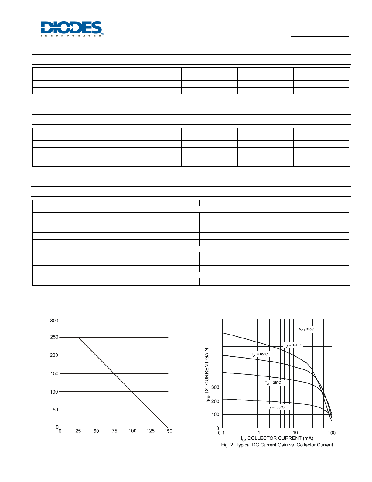
Fig. 1 Power Di s sipation vs. Ambient Temperatu r e ( N ote 4)
R = 500 C/W
°
θ
JA
T , AMBIENT TEMPERATURE (°C)
A
DDTC113TLP
Document number: DS30843 Rev. 8 - 2
2 of 4
www.diodes.com
February 2011
© Diodes Incorporated
 Loading...