Diodes DDTC113TCA, DDTC114TCA, DDTC115TCA, DDTC123TCA, DDTC124TCA Schematic [ru]
...
–
NPN PRE-BIASED SMALL SIGNAL SURFACE MOUNT TRANSISTOR
Features
Epitaxial Planar Die Construction
Complementary PNP Types Available (DDTA)
Built-In Biasing Resistors, R1only
Totally Lead-Free & Fully RoHS compliant (Notes 1 & 2)
Halogen and Antimony Free "Green" Device (Note 3)
Qualified to AEC-Q101 Standards for High Reliability
PPAP Capable (Note 4)
Part Number R1 (NOM)
DDTC113TCA 1KΩ
DDTC123TCA 2.2KΩ
DDTC143TCA 4.7KΩ
DDTC114TCA 10KΩ
DDTC124TCA 22KΩ
DDTC144TCA 47KΩ
DDTC115TCA 100KΩ
DDTC125TCA 200KΩ
SOT23
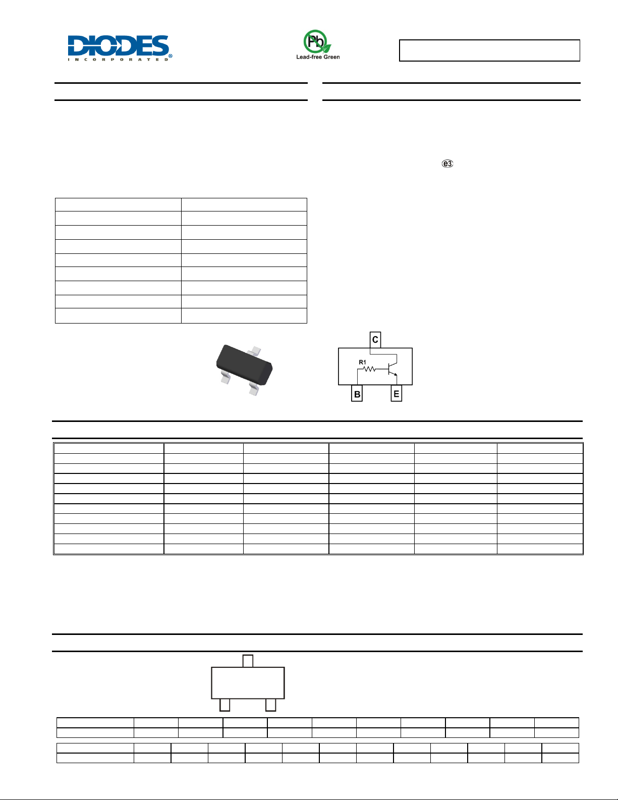
Top View
DDTC(R1-ONLY SERIES) CA
Mechanical Data
Case: SOT23
Case Material: Molded Plastic, “Green” Molding Compound
UL Flammability Classification Rating 94V-0
Moisture Sensitivity: Level 1 per J-STD-020
Terminals: Finish – Matte Tin Plated Leads, Solderable per
MIL-STD-202, Method 208
Weight: 0.008 grams (approximate)
Device Schematic
Top View
Ordering Information (Notes 4 & 5)
Product Compliance Marking Reel size (inches) Tape width (mm) Quantity per reel
DDTC113TCA-7-F AEC-Q101 N01 7 8 3,000
DDTC123TCA-7-F AEC-Q101 N03 7 8 3,000
DDTC143TCA-7-F AEC-Q101 N07 7 8 3,000
DDTC143TCAQ-7-F Automotive N07 7 8 3,000
DDTC143TCAQ-13-F Automotive N07 13 8 10,000
DDTC114TCA-7-F AEC-Q101 N12 7 8 3,000
DDTC124TCA-7-F AEC-Q101 N16 7 8 3,000
DDTC144TCA-7-F AEC-Q101 N19 7 8 3,000
DDTC115TCA-7-F AEC-Q101 N23 7 8 3,000
DDTC125TCA-7-F AEC-Q101 N25 7 8 3,000
Notes: 1. No purposely added lead. Fully EU Directive 2002/95/EC (RoHS) & 2011/65/EU (RoHS 2) compliant.
2. See http://www.diodes.com/quality/lead_free.html for more information about Diodes Incorporated’s definitions of Halogen- and Antimony-free, "Green"
and Lead-free.
3. Halogen- and Antimony-free "Green” products are defined as those which contain <900ppm bromine, <900ppm chlorine (<1500ppm total Br + Cl) and
<1000ppm antimony compounds.
4. Automotive products are AEC-Q101 qualified and are PPAP capable. Automotive, AEC-Q101 and standard products are electrically and thermally the
same, except where specified. For more information, please refer to http://www.diodes.com/quality/product_compliance_definitions/.
5. For packaging details, go to our website at http://www.diodes.com/products/packages.html.
Marking Information
Date Code Key
Year 2006 2007 2008 2009 2010 2011 2012 2013 2014 2015
Code T U V W X Y Z A B C
Month Jan Feb Mar Apr May Jun Jul Aug Sep Oct Nov Dec
Code 1 2 3 4 5 6 7 8 9 O N D
Nxx
DDTC(R1-ONLY SERIES) CA
Document number: DS30331 Rev. 9 - 2
NXX = Product Type Marking Code (See Table above)
YM = Date Code Marking
YM
Y = Year (ex: X = 2010)
M = Month (ex: 9 = September)
1 of 5
www.diodes.com
November 2013
© Diodes Incorporated

Absolute Maximum Ratings (@T
= +25°C, unless otherwise specified.)
A
Characteristic Symbol Value Unit
Collector-Base Voltage
Collector-Emitter Voltage
Emitter-Base Voltage
Collector Current
I
C
Thermal Characteristics (@T
= +25°C, unless otherwise specified.)
A
Characteristic Symbol Value Unit
Power Dissipation (Note 6)
Thermal Resistance, Junction to Ambient Air (Note 6)
Operating and Storage Temperature Range
Electrical Characteristics (@T
= +25°C, unless otherwise specified.)
A
T
Characteristic Symbol Min Typ Max Unit Test Condition
Collector-Base Breakdown Voltage
Collector-Emitter Breakdown Voltage
Emitter-Base Breakdown Voltage
Collector Cutoff Current
Emitter Cutoff Current
Collector-Emitter Saturation Voltage
DC Current Transfer Ratio
BV
CBO
BV
CEO
BV
EBO
I
CBO
I
EBO
V
CE(sat)
h
FE
Input Resistor (R1) Tolerance R1
Gain-Bandwidth Product (Note 7)
Notes: 6. Mounted on FR4 PC Board with minimum recommended pad layout
7. Transistor - For Reference Only
f
T
50
50
5
100
120
-30
V
CBO
V
CEO
V
EBO
(Max)
P
D
R
θJA
, T
J
STG
0.5 μA
0.5 μA
0.3 V
250 - 600
630
+30 %
250
DDTC(R1-ONLY SERIES) CA
50 V
50 V
5 V
100 mA
200 mW
625 °C/W
-55 to +150 °C
V
IC = 50μA
V
IC = 1mA
V
IE = 50μA
VCB = 50V
VEB = 4V
= 10mA/1mA DDTC113TCA
I
C/IB
= 5mA/0.5mA DDTC123TCA
I
C/IB
I
= 2.5mA/.25mA DDTC143TCA
C/IB
= 1mA/.1mA DDTC114TCA
I
C/IB
I
= 5mA/0.5mA DDTC124TCA
C/IB
= 2.5mA/.25mA DDTC144TCA
I
C/IB
I
= 1mA/0.1mA DDTC115TCA
C/IB
I
= .5mA/.05mA DDTC125TCA
C/IB
= 1mA, VCE = 5V
I
C
I
= 5mA, VCE = 5V DDTC143TCAQ
C
= 10V, IE = -5mA,
V
CE
MHz
f = 100MHz
DDTC(R1-ONLY SERIES) CA
Document number: DS30331 Rev. 9 - 2
2 of 5
www.diodes.com
November 2013
© Diodes Incorporated
 Loading...