Diodes DDTB113EC, DDTB113ZC, DDTB114EC, DDTB114GC, DDTB114TC Schematic [ru]
...
Please click here to visit our online spice models database.
Features
• Epitaxial Planar Die Construction
• Complementary NPN Types Available (DDTD)
• Built-In Biasing Resistors, R1, R2
• Lead, Halogen and Antimony Free, RoHS Compliant
"Green" Device (Notes 2 and 3)
Mechanical Data
• Case: SOT-23
• Case Material: Molded Plastic. UL Flammability
Classification Rating 94V-0
• Moisture Sensitivity: Level 1 per J-STD-020D
NEW PRODUCT
• Terminal Connections: See Diagram
• Terminals: Solderable per MIL-STD-202, Method 208
• Lead Free Plating (Matte Tin Finish annealed over Alloy
42 leadframe)
• Marking Information: See Table Below & Page 3
• Ordering Information: See Page 3
• Weight: 0.008 grams (approximate)
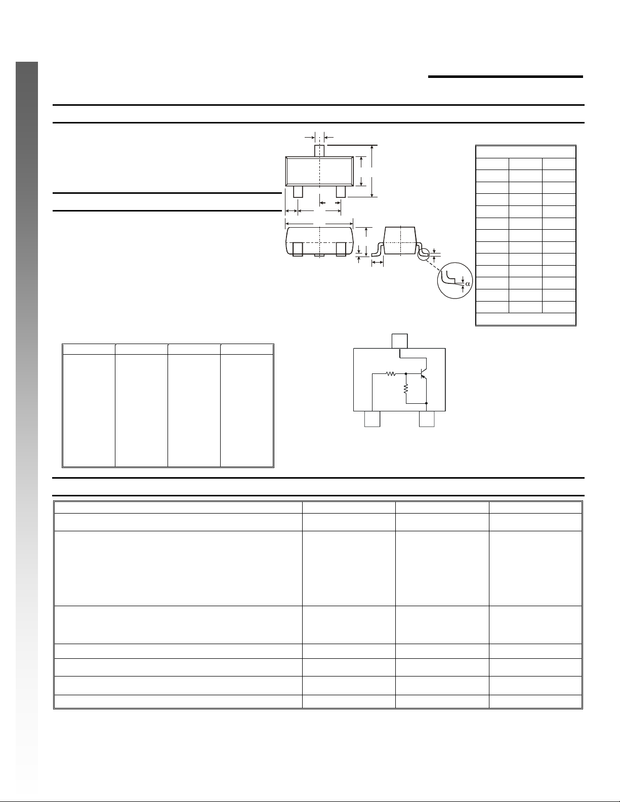
P/N R1 (NOM) R2 (NOM) Type Code
DDTB113EC
DDTB123EC
DDTB143EC
DDTB114EC
DDTB122JC
DDTB113ZC
DDTB123YC
DDTB133HC
DDTB123TC
DDTB143TC
DDTB114TC
DDTB114GC
1K
2.2K
4.7K
10K
0.22K
1K
2.2K
3.3K
2.2K
4.7K
10K
0
1K
2.2K
4.7K
10K
4.7K
10K
10K
10K
OPEN
OPEN
OPEN
10K
P60
P61
P62
P63
P64
P65
P66
P67
P69
P70
P71
P72
DDTB (xxxx) C
PNP PRE-BIASED 500 mA SURFACE MOUNT TRANSISTOR
SOT-23
0° 8°
E
TOP VIEW
G
H
A
D
B
C
K
J
Schematic and Pin Configuration
L
OUT
3
C
R1
B
R2
IN
GND(+)
Dim Min Max
A 0.37 0.51
B 1.20 1.40
C 2.30 2.50
D 0.89 1.03
E 0.45 0.60
M
E
21
G 1.78 2.05
H 2.80 3.00
J 0.013 0.10
K 0.903 1.10
L 0.45 0.61
M 0.085 0.180
α
All Dimensions in mm
Maximum Ratings @T
Characteristic Symbol Value Unit
Supply Voltage, (3) to (2)
Input Voltage, (1) to (2) DDTB113EC
DDTB123EC
DDTB143EC
DDTB114EC
DDTB122JC
DDTB113ZC
DDTB123YC
DDTB133HC
Input Voltage, (1) to (2) DDTB123TC
DDTB143TC
DDTB114TC
DDTB114GC
Output Current All
Power Dissipation
Thermal Resistance, Junction to Ambient Air (Note 1)
Operating and Storage Temperature Range
Notes: 1. Mounted on FR4 PC Board with recommended pad layout at http://www.diodes.com/datasheets/ap02001.pdf.
DS30385 Rev. 7 - 2
2. No purposefully added lead. Halogen and Antimony Free.
3. Product manufactured with Data Code V9 (week 33, 2008) and newer are built with Green Molding Compound. Product manufactured prior to Date
Code V9 are built with Non-Green Molding Compound and may contain Halogens or Sb
= 25°C unless otherwise specified
A
VCC
VIN
V
EBO (MAX)
IC
PD
R
JA
θ
TJ, T
1 of 3
www.diodes.com
STG
-50 V
+10 to -10
+10 to -12
+10 to -30
+10 to -40
+5 to -5
+5 to -10
+5 to -12
+6 to -20
Fire Retardants.
2O3
-5 V
-500 mA
200 mW
625
-55 to +150
V
°C/W
°C
DDTB (xxxx) C
© Diodes Incorporated

Electrical Characteristics @T
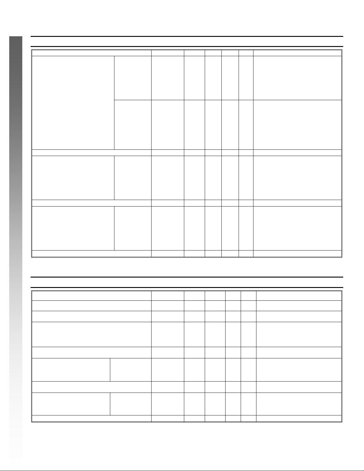
Characteristic Symbol Min Typ Max Unit Test Condition
Input Voltage
Output Voltage
NEW PRODUCT
Input Current
Output Current
DC Current Gain
Gain-Bandwidth Product*
* Transistor - For Reference Only
= 25°C unless otherwise specified R1, R2 Types
A
DDTB113EC
DDTB123EC
DDTB143EC
DDTB114EC
DDTB122JC
DDTB113ZC
DDTB123YC
DDTB133HC
DDTB113EC
DDTB123EC
DDTB143EC
DDTB114EC
DDTB122JC
DDTB113ZC
DDTB123YC
DDTB133HC
DDTB113EC
DDTB123EC
DDTB143EC
DDTB114EC
DDTB122JC
DDTB113ZC
DDTB123YC
DDTB133HC
DDTB113EC
DDTB123EC
DDTB143EC
DDTB114EC
DDTB122JC
DDTB113ZC
DDTB123YC
DDTB133HC
V
l(off)
V
l(on)
V
O(on)
Il ⎯ ⎯
I
O(off)
Gl
fT ⎯
-0.5
-0.5
-0.5
-0.5
-0.5
⎯ ⎯
-0.3
-0.3
-0.3
⎯ ⎯
⎯ ⎯
⎯ ⎯
33
39
47
56
47
⎯ ⎯ ⎯ VO = -5V, IO = -50mA
56
56
56
200
V
-3.0
-3.0
-3.0
-3.0
-3.0
V
-2.0
-2.0
-2.0
-0.3V V
-7.2
-3.8
-1.8
-0.88
mA
-28
-7.2
-3.6
-2.4
-0.5
μA
MHz
⎯
VCC = -5V, IO = -100μA
VO = -0.3V, IO = -20mA
VO = -0.3V, IO = -20mA
VO = -0.3V, IO = -20mA
VO = -0.3V, IO = -10mA
VO = -0.3V, IO = -30mA
VO = -0.3V, IO = -20mA
VO = -0.3V, IO = -20mA
VO = -0.3V, IO = -20mA
IO/Il = -50mA/-2.5mA
VI = -5V
VCC = -50V, VI = 0V
VCE = -10V, IE = -5mA, f = 100MHz
Electrical Characteristics @T
= 25°C unless otherwise specified R1-Only, R2-Only Types
A
Characteristic Symbol Min Typ Max Unit Test Condition
Collector-Base Breakdown Voltage
Collector-Emitter Breakdown Voltage
Emitter-Base Breakdown Voltage DDTB123TC
DDTB143TC
DDTB114TC
DDTB114GC
Collector Cutoff Current
DDTB123TC
Emitter Cutoff Current
DDTB143TC
DDTB114TC
DDTB114GC
Collector-Emitter Saturation Voltage
DDTB123TC
DC Current Transfer Ratio
DDTB143TC
DDTB114TC
DDTB114GC
Gain-Bandwidth Product*
* Transistor - For Reference Only
DS30385 Rev. 7 - 2
BV
CBO
BV
CEO
BV
EBO
I
⎯ ⎯
CBO
I
EBO
-300
V
CE(sat)
hFE
fT ⎯
2 of 3
www.diodes.com
-50
-40
-5
⎯
⎯
⎯
⎯ ⎯
100
100
100
56
⎯ ⎯
⎯ ⎯
⎯ ⎯
⎯
250
250
250
⎯
200
-0.5
-0.5
-0.5
-0.5
-580
-0.3 V
600
600
600
⎯
MHz
⎯
V
IC = -50μA
V
IC = -1mA
IE = -50μA
IE = -50μA
V
IE = -50μA
IE = -720μA
μA
VCB = -50V
μA
VEB = -4V
IC = -50mA, IB = -2.5mA
⎯
IC = -5mA, VCE = -5V
VCE = -10V, IE = 5mA, f = 100MHz
DDTB (xxxx) C
© Diodes Incorporated
 Loading...