

Diodes DCX-LO-R1-U User Manual
COMPLEMENTARY NPN/PNP PRE-BIASED SMALL SIGNAL DUAL SURFACE MOUNT TRANSISTOR
Features
• Epitaxial Planar Die Construction
• Built-In Biasing Resistors
• Lead Free/RoHS Compliant (Note 3)
• "Green" Device (Note 4 and 5)
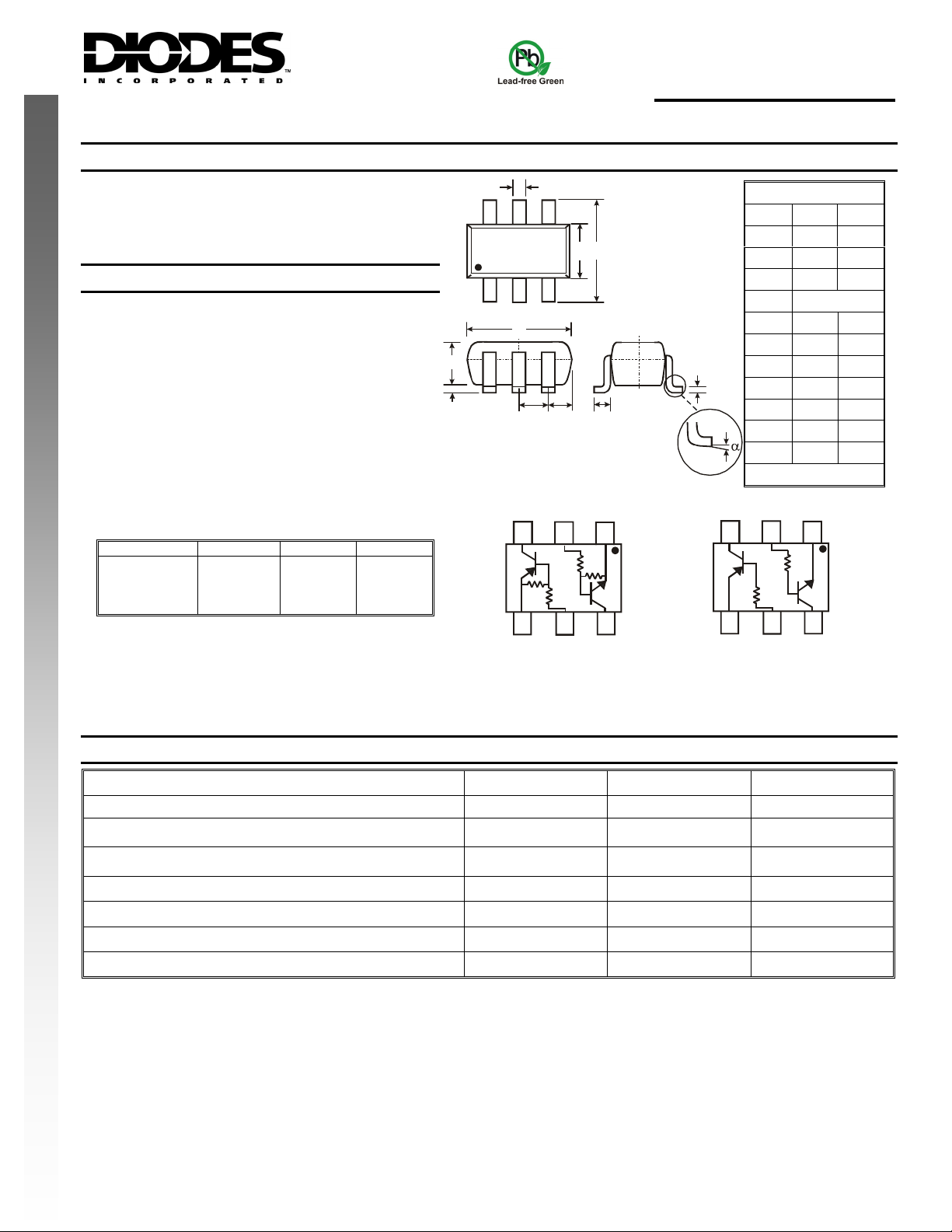
Mechanical Data
• Case: SOT-363
• Case Material: Molded Plastic. UL Flammability
Classification Rating 94V-0
• Moisture Sensitivity: Level 1 per J-STD-020C
• Terminals: Finish - Matte Tin Solderable per MIL-STD-
202, Method 208
• Lead Free Plating (Matte Tin Finish annealed over Alloy
NE P DUCP DUCW RO T T RO
42 leadframe).
• Terminal Connections: See Diagram
• Marking Information: See Page 4
• Type Code: See Table Below
• Ordering Information: See Page 4
• Weight: 0.006 grams (approximate)
P/N R1 (NOM) R2 (NOM) Type Code
DCX122LU
DCX142JU
DCX122TU
DCX142TU
0.22K
0.47K
0.22K
0.47K
10K
10K
OPEN
OPEN
C81
C82
C83
C84
DCX (LO-R1) UDCX (LO-R1) U
K
J
A
CXX YM
H
D
R
SOT-363
Dim Min Max
C
B
M
L
F
R
R
1
2
R
2
1
R1, R2 R
SCHEMATIC DIAGRAM
A 0.10 0.30
B 1.15 1.35
C 2.00 2.20
D 0.65 Nominal
F 0.30 0.40
H 1.80 2.20
J
K 0.90 1.00
L 0.25 0.40
M 0.10 0.25
α
All Dimensions in mm
R
1
R
1
Only
1
⎯
0°
0.10
8°
Maximum Ratings NPN Section @T
Characteristic Symbol Value Unit
Supply Voltage
Input Voltage DCX122LU
DCX142JU
Input Voltage DCX122TU
DCX142TU
Output Current All
Power Dissipation (Note 1, 2)
Thermal Resistance, Junction to Ambient Air (Note 2)
Operating and Storage Temperature Range
Notes: 1. Mounted on FR4 PC Board with recommended pad layout at http://www.diodes.com/datasheets/ap02001.pdf.
2. 150mW per element must not be exceeded.
3. No purposefully added lead.
4. Diodes Inc.'s "Green" policy can be found on our website at http://www.diodes.com/products/lead_free/index.php.
5. Product manufactured with Date Code UO (week 40, 2007) and newer are built with Green Molding Compound. Product manufactured prior to Date
Code UO are built with Non-Green Molding Compound and may contain Halogens or Sb2O3 Fire Retardants.
DS30425 Rev. 5 - 2
= 25°C unless otherwise specified
A
VCC
VIN
V
EBO (MAX)
Tj, T
1 of 4
www.diodes.com
IC
Pd
R
JA
θ
STG
-5 to +6
-5 to +6
-55 to +150
50 V
V
5 V
100 mA
200 mW
625
°C/W
°C
DCX (LO-R1) U
© Diodes Incorporated

Maximum Ratings PNP Section @T
Characteristic Symbol Value Unit
Supply Voltage
Input Voltage DCX122LU
DCX142JU
Input Voltage DCX122TU
DCX142TU
Output Current All
Power Dissipation (Note 1,2)
Thermal Resistance, Junction to Ambient Air (Note 1,2)
Operating and Storage Temperature Range
NEW PRODUCT
Electrical Characteristics NPN Section @T
Characteristic Symbol Min Typ Max Unit Test Condition
DCX122LU
Input Voltage
Output Voltage
Input Current
Output Current
DC Current Gain
Gain-Bandwidth Product*
* Transistor - For Reference Only
DCX142JU
DCX122LU
DCX142JU
DCX122LU
DCX142JU
DCX122LU
DCX142JU
= 25°C unless otherwise specified
A
VCC
VIN
V
EBO (MAX)
IC
Pd
R
JA
θ
Tj, T
STG
= 25°C unless otherwise specified R1, R2 Types
A
V
l(off)
V
⎯ ⎯
l(on)
V
O(on)
Il ⎯ ⎯
I
O(off)
Gl
fT
0.3
0.3
⎯ ⎯
⎯ ⎯
⎯ ⎯
56
56
⎯
⎯ ⎯ ⎯ VO = 5V, IO = 10mA
200
2.0
2.0
0.3V V
28
13
0.5
⎯
-50 V
+5 to -6
+5 to -6
-5 V
-100 mA
200 mW
625
-55 to +150
V
VCC = 5V, IO = 100μA
VO = 0.3V, IO = 20mA
V
VO = 0.3V, IO = 20mA
IO/Il = 5mA/0.25mA
mA
VI = 5V
μA
VCC = 50V, VI = 0V
MHz
VCE = 10V, IE = 5mA, f = 100MHz
V
°C/W
°C
Electrical Characteristics NPN Section @T
Characteristic Symbol Min Typ Max Unit Test Condition
Collector-Base Breakdown Voltage
Collector-Emitter Breakdown Voltage
Emitter-Base Breakdown Voltage DCX122TU
DCX142TU
Collector Cutoff Current
Emitter Cutoff Current
DCX122TU
DCX142TU
Collector-Emitter Saturation Voltage
DC Current Transfer Ratio
DCX122TU
DCX142TU
Gain-Bandwidth Product*
* Transistor - For Reference Only
BV
CBO
BV
CEO
BV
EBO
I
CBO
I
EBO
V
⎯ ⎯
CE(sat)
hFE
fT
DS30425 Rev. 5 - 2
www.diodes.com
= 25°C unless otherwise specified R1 Only
A
50
40
5
⎯ ⎯
⎯
⎯
100
100
⎯
⎯ ⎯
⎯ ⎯
⎯ ⎯
⎯
250
250
200
V
IC = 50μA
V
IC = 1mA
IE = 50μA
V
IE = 50μA
0.5
μA
VCB = 50V
0.5
μA
0.5
0.3 V
600
600
⎯
VEB = 4V
IC = 5mA, IB = 0.25mA
⎯ IC = 1mA, VCE = 5V
MHz
VCE = 10V, IE = -5mA, f = 100MHz
2 of 4
DCX (LO-R1) U
© Diodes Incorporated
 Loading...