Diodes DCP69 User Manual

g
Features
• Epitaxial Planar Die Construction
• Complementary NPN Type Available (DCP68)
• Ideally Suited for Automated Assembly Processes
• Ideal for Medium Power Switching or Amplification Applications
• Totally Lead-Free & Fully RoHS compliant (Note 1)
• Halogen and Antimony Free. “Green” Device (Note 2)
• Qualified to AEC-Q101 Standards for High Reliability
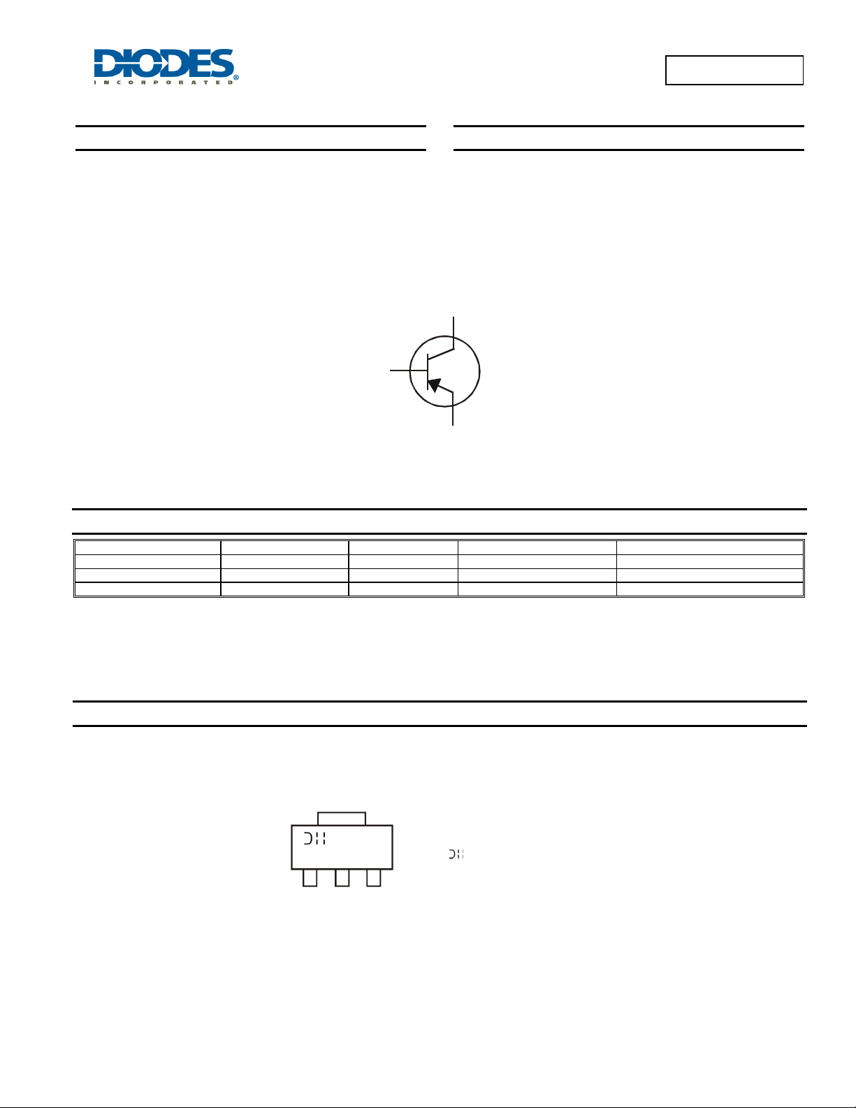
SOT223
Top View
B
Device Schematic
DCP69/-16/-25
20V PNP SURFACE MOUNT TRANSISTOR
Mechanical Data
• Case: SOT223
• Case Material: Molded Plastic, "Green Molding” Compound.
UL Flammability Classification Rating 94V-0
• Moisture Sensitivity: Level 1 per J-STD-020
• Terminals: Finish - Matte Tin
• Solderable per MIL-STD -202, Method 208
• Weight: 0.112 grams (approximate)
C
E
Top View
Pin Out Confi
uration
Ordering Information (Note 3)
Part Number
DCP69-13 P12 13 12 2500
DCP69-16-13 P12-16 13 12 2500
DCP69-25-13 P12-25 13 12 2500
Notes: 1. No purposely added lead. Fully EU Directive 2002/95/EC (RoHS) & 2011/65/EU (RoHS 2) compliant.
2. Halogen and Antimony free "Green” products are defined as those which contain <900ppm bromine, <900ppm chlorine (<1500ppm total Br + Cl) and
<1000ppm antimony compounds.
3. For packaging details, go to our website at http://www.diodes.com.
Marking Reel size (inches) Tape width (mm) Quantity per reel
Marking Information
W
W
Y
xxx
xxx = Product Type Marking Code
P12 = DCP69
P12-16 = DCP69-16
P12-25 = DCP69-25
= Manufacturer’s code marking
YWW = Date Code Marking
Y = Last digit of year (ex: 1 = 2011)
WW = Week code (01 – 53)
DCP69/-16/-25
Document number: DS30798 Rev. 7 - 2
1 of 5
www.diodes.com
April 2012
© Diodes Incorporated

θ
θ
)
Maximum Ratings @T
= 25°C unless otherwise specified
A
Characteristic Symbol Value Units
Collector-Base Voltage
Collector-Emitter Voltage
Emitter-Base Voltage
Collector Current
Peak Pulse Current
Thermal Characteristics @T
= 25°C unless otherwise specified
A
Characteristic Symbol Value Unit
Power Dissipation (Note 4)
Thermal Resistance, Junction to Ambient Air (Note 4)
Power Dissipation (Note 5)
Thermal Resistance, Junction to Ambient Air (Note 5)
Operating and Storage Temperature Range
DCP69/-16/-25
V
CBO
V
CEO
V
EBO
I
C
I
CM
P
D
R
JA
P
D
R
JA
T
, T
J
STG
-25 V
-20 V
-5.0 V
-1.0 A
-2.0 A
1 W
125 °C/W
2 W
62.5 °C/W
-55 to +150 °C
Electrical Characteristics @T
= 25°C unless otherwise specified
A
Characteristic Symbol Min Typ Max Unit Test Condition
OFF CHARACTERISTICS
Collector-Base Breakdown Voltage
Collector-Emitter Breakdown Voltage (Note 6)
Emitter-Base Breakdown Voltage
Collector-Base Cutoff Current
Emitter-Base Cutoff Current
BV
BV
BV
I
CBO
I
EBO
CBO
CEO
EBO
-25 — — V
-20 — — V
-5.0 — — V
— —
— — -100 nA
-100
-10
IC = -100μA, IE = 0
IC = -10mA, IB = 0
IE = -100μA, IC = 0
nA
V
CB
μA
V
CB
VEB = -5.0V, IC = 0
= -25V, IE = 0
= -25V, IE = 0, TA = 150°C
ON CHARACTERISTICS (Note 6)
V
DCP69, DCP69-16, DCP69-25
DC Current Gain
Collector-Emitter Saturation Voltage
Base-Emitter Turn-On Voltage
50
60
DCP69 85 — 375
h
FE
—
—
—
—
DCP69-16 100 — 250
DCP69-25 160 — 375
V
CE(sat
V
BE (on)
— — -0.5 V
— —
-0.7
-1.0
—
V
= -10V, IC = -5.0mA
CE
V
= -1.0V, IC = -1.0A
CE
V
= -1.0V, IC = -500mA
CE
V
= -1.0V, IC = -500mA
CE
V
= -1.0V, IC = -500mA
CE
IC = -1.0A, IB = -100mA
= -10V, IC = -5.0mA
V
CE
= -1.0V, IC = -1.0A
V
CE
SMALL SIGNAL CHARACTERISTICS
Current Gain-Bandwidth Product
Output Capacitance
Notes: 4. Device mounted on FR-4 PCB; pad layout as shown on in Diodes Inc. suggested pad layout document, which can be found on our website at
6. Measured under pulsed conditions. Pulse width = 300μS. Duty cycle ≤ 2%.
http://www.diodes.com
5. Device mounted on FR-4 PCB with 1in.
2
copper pad layout
f
T
C
obo
40 200 — MHz
— 17 — pF
VCE = -5.0V, IC = -50mA, f = 100MHz
VCB = -10V, f = 1 MHz
DCP69/-16/-25
Document number: DS30798 Rev. 7 - 2
2 of 5
www.diodes.com
April 2012
© Diodes Incorporated
 Loading...