Diodes D5V0L1B2WS User Manual

Features
• Provides ESD Protection per IEC 61000-4-2 Standard:
Air – ±30kV, Contact – ±30kV
• 1 Channel of ESD Protection
• Low Channel Input Capacitance
• Typically Used in Cellular Handsets, Portable Electronics,
Communication Systems, Computers and Peripherals
• Lead Free/RoHS Compliant (Note 1)
• “Green” Device (Note 2)
ADVANCE INFORMATION
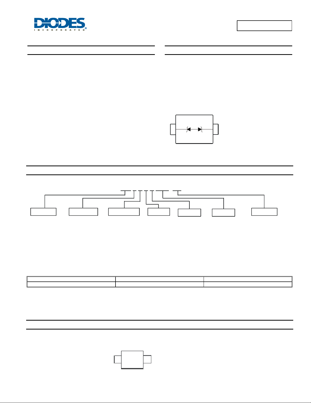
Top View
Ordering Information (Note 3)
D5V0L1B2WS
LOW CAPACITANCE BIDIRECTIONAL TVS DIODE
Mechanical Data
• Case: SOD323
• Case Material: Molded Plastic, “Green” Molding Compound. UL
Flammability Classification Rating 94V-0
• Moisture Sensitivity: Level 1 per J-STD-020
• Terminals: Matte Tin Finish annealed over Alloy 42 leadframe
(Lead Free Plating). Solderable per MIL-STD-202, Method 208
• Weight: 0.004 grams (approximate)
1
Device Schematic
2
Voltage Capacitance # of Channels Polarity # of Pins Package Packing
5V0: 5.0 Volts
Notes: 1. EU Directive 2002/95/EC (RoHS) & 2011/65/EU (RoHS 2) compliant. No purposely added lead. Halogen and Antimony free.
X: Extremely Low (<0.5pF)
F: Ultra Low (0.5 ~ 1.0pF)
P: Very Low (1.1 ~ 10pF)
L: Low (1 0. 1 ~ 20pF)
M: Medium (>20pF)
Part Number Case Packaging
D5V0L1B2WS-7 SOD323 3000/Tape & Reel
2. Diodes Inc.’s “Green” policy can be found on our website at http://www.diodes.com.
3. For packaging details, go to our website at http://www.diodes.com.
D 5V0 L X B X XXX- XX
1: 1 Chann e l
2: 2 Chann els
4: 4 Chann els
6: 6 Chann els
B: Bidirectional
(Symmetrical)
U: Unidirecti on al
A: Bidirectional
(Asymmetrical)
2: 2 Pins
3: 3 Pins
5: 5 Pins
6: 6 Pins
8: 8 Pins
10: 10 Pins
LP3: X3-D FN0603- 2
LP: X1-DFN1006-2
LP4: X2-D FN1006- 2
WS: SOD323
T: SOD523/SOT523
SO: SOT23/SOT2 5
W: SOD123/SOT323
TS: TSOT25/TSOT26
S: SOT353/SOT363
V:SOT553/SOT563
7B: 7” reel (10Kreel)
Marking Information
D5V0L1B2WS
Document number: DS35429 Rev. 4 - 2
NN
NN = Product Type Marking Code
1 of 4
www.diodes.com
7: 7” reel (3K/reel)
13: 13” reel
January 2012
© Diodes Incorporated

t
r
θ
C, TOT
C
PACITANC
Maximum Ratings @T
= 25°C unless otherwise specified
A
Characteristic Symbol Value Unit Conditions
Peak Pulse Power Dissipation
Peak Pulse Current
ESD Protection – Contact Discharge
ESD Protection – Air Discharge
Thermal Characteristics
Characteristic Symbol Value Unit
Package Power Dissipation (Note 4)
Thermal Resistance, Junction to Ambient (Note 4)
Operating and Storage Temperature Range
ADVANCE INFORMATION
P
I
PP
V
ESD_Contac
V
ESD_Ai
PP
D5V0L1B2WS
84 W
6 A
±30 kV Standard IEC 61000-4-2
±30 kV Standard IEC 61000-4-2
P
D
R
JA
, T
T
J
STG
-65 to +150
8/20μs, Per Fig. 1
8/20μs, Per Fig. 1
200 mW
625
°C/W
°C
Electrical Characteristics @T
= 25°C unless otherwise specified
A
Characteristic Symbol Min Typ Max Unit Test Conditions
Reverse Standoff Voltage
Channel Leakage Current (Note 5)
Clamping Voltage, Positive Transients
Breakdown Voltage
Differential Resistance
Channel Input Capacitance
Notes: 4. Device mounted on FR-4 PCB pad layout (2oz copper) as shown on Diodes, Inc. suggested pad layout AP02001, which can be found on our website at
http://www.diodes.com.
5. Short duration pulse test used to minimize self-heating effect.
V
RWM
I
V
V
R
C
RM
CL
BR
DIF
T
- - 5 V -
- 10 100 nA
-
-
-
-
7.0
8.7
10.5
11.5
9.0
10.7
12.0
14.0
6 7 8 V
-
0.2 -
- 15 20 pF
V
RWM
I
PP
I
PP
V
I
PP
I
PP
IR = 1mA
Ω
I
R
VR = 0V, f = 1MHz
= 5V
= 1A, tp = 8/20μS
= 3A, tp = 8/20μS
= 5A, tp = 8/20μS
= 6A, tp = 8/20μS
= 1A, tp = 8/20μS
18
17
f = 1MHz
100
16
E (pF)
15
14
50
A
13
AL
12
T
PppP
I , PEAK PULSE CURRENT (%I )
0
0
20 40
t, TIME ( s)
μ
60
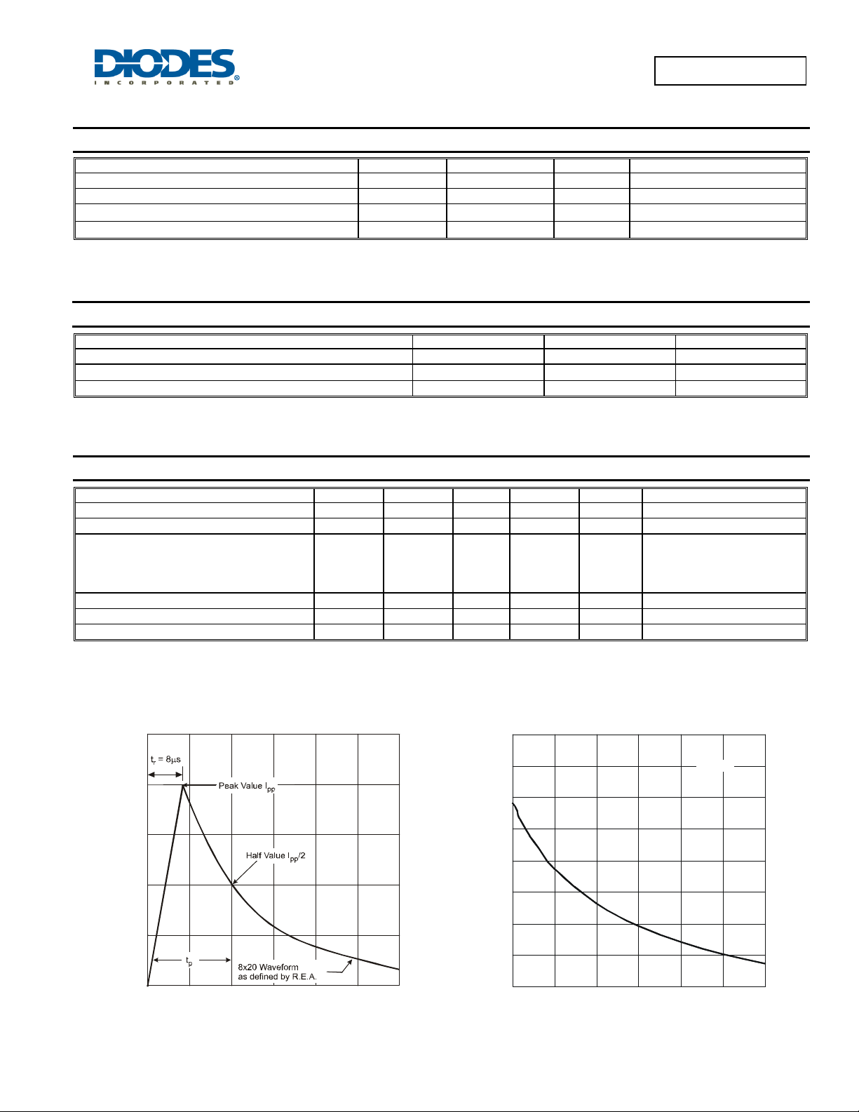
Fig. 1 Pulse Waveform
11
10
01 23 456
Fig. 2 Typ ic al Total Capacitance vs. Revers e Vol tage
V , REVERSE VOL TAGE (V)
R
D5V0L1B2WS
Document number: DS35429 Rev. 4 - 2
2 of 4
www.diodes.com
January 2012
© Diodes Incorporated
 Loading...