

Page 1
W
Please click here to visit our online spice models database.
Features
• Planar Die Construction
• 200mW Power Dissipation
• Zener Voltages from 2.4V – 39V
• Ultra-Small Surface Mount Package
• Lead Free/RoHS Compliant (Note 4)
• "Green" Device (Notes 1 and 2)
Maximum Ratings @T
Characteristic Symbol Value Unit
Forward Voltage @ I
= 25°C unless otherwise specified
A
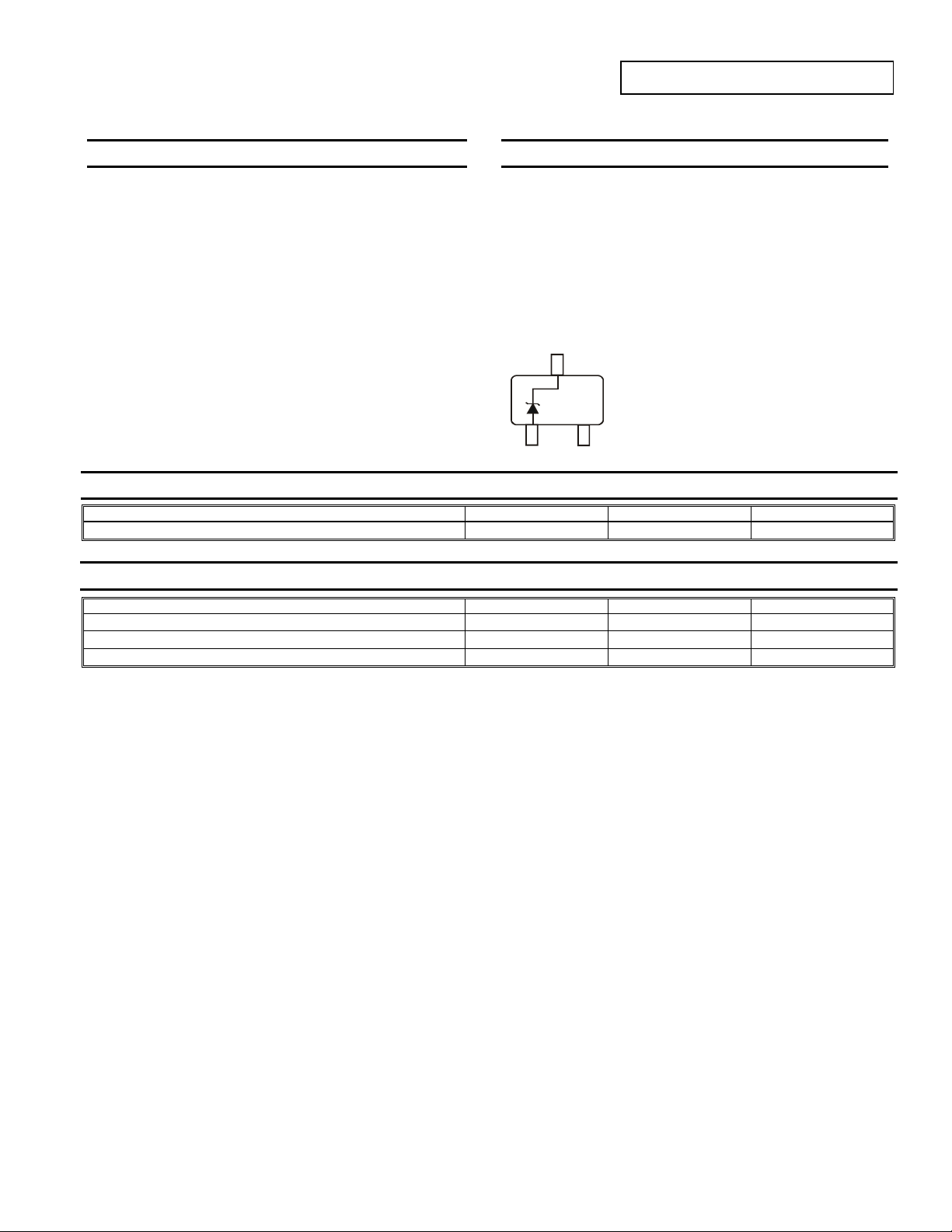
Top View
10mA VF
F =
BZX84C2V4W - BZX84C39
200mW SURFACE MOUNT ZENER DIODE
Mechanical Data
• Case: SOT-323
• Case Material: Molded Plastic, "Green" Molding Compound,
Note 2. UL Flammability Classification Rating 94V-0
• Moisture Sensitivity: Level 1 per J-STD-020D
• Terminals: Solderable per MIL-STD-202, Method 208
• Lead Free Plating (Matte Tin Finish annealed over Alloy 42
leadframe).
• Polarity: See Diagram
• Marking Information: See Page 3
• Ordering Information: See Page 3
• Weight: 0.006 grams (approximate)
Device Schematic
0.9 V
Thermal Characteristics
Characteristic Symbol Value Unit
Power Dissipation (Note 3)
Thermal Resistance, Junction to Ambient Air (Note 3)
Operating and Storage Temperature Range
Notes: 1. Diodes Inc.'s "Green" policy can be found on our website at http://www.diodes.com./products/lead_free/index.php.
Code 0627 are built with Non-Green Molding Compound and may contain Halogens or Sb2O3 Fire Retardants.
2. Product manufactured with Date Code 0627 (week 27, 2006) and newer are built with Green Molding Compound. Product manufactured prior to Date
3. Mounted on FR4 PC board with recommended pad layout which can be found on our website at http://www.diodes.com/datasheets/ap02001.pdf.
4. No purposefully added lead.
R
TJ, T
PD
θ
JA
STG
200 mW
625 K/W
-65 to +125
°C
BZX84C2V4W - BZX84C39W
Document number: DS30066 Rev. 15 - 2
1 of 4
www.diodes.com
May 2008
© Diodes Incorporated
Page 2
W
P, P
O
R
PATIO
NER
CUR
R
N
T
BZX84C2V4W - BZX84C39
Electrical Characteristics @T
Type Number
Marking
Code
Nom (V) Min (V) Max (V) mA
= 25°C unless otherwise specified
A
Zener Voltage
Maximum Zener Impedance
Range (Note 5)
VZ @ IZT I
ZZT @ IZTZZK @ IZK IZK IR @ VR
ZT
(Note 6)
Ω
Maximum
Reverse Current
(Note 5)
Temperature
Coefficient of
Zener Voltage
@ I
5mA
ZT =
(mV/°C)
mA uA V Min Max
BZX84C2V4W KRB 2.4 2.2 2.6 5.0 100 600 1.0 50 1.0 -3.5 0
BZX84C2V7W KRC 2.7 2.5 2.9 5.0 100 600 1.0 20 1.0 -3.5 0
BZX84C3V0W KRD 3.0 2.8 3.2 5.0 95 600 1.0 20 1.0 -3.5 0
BZX84C3V3W KRE 3.3 3.1 3.5 5.0 95 600 1.0 5.0 1.0 -3.5 0
BZX84C3V6W KRF 3.6 3.4 3.8 5.0 90 600 1.0 5.0 1.0 -3.5 0
BZX84C3V9W KRG 3.9 3.7 4.1 5.0 90 600 1.0 3.0 1.0 -3.5 0
BZX84C4V3W KRH 4.3 4.0 4.6 5.0 90 600 1.0 3.0 1.0 -3.5 0
BZX84C4V7W KR1 4.7 4.4 5.0 5.0 80 600 1.0 3.0 2.0 -3.5 0.2
BZX84C5V1W KR2 5.1 4.8 5.4 5.0 60 500 1.0 2.0 2.0 -2.7 1.2
BZX84C5V6W KR3 5.6 5.2 6.0 5.0 40 480 1.0 1.0 2.0 -2.0 2.5
BZX84C6V2W KR4 6.2 5.8 6.6 5.0 10 400 1.0 3.0 4.0 0.4 3.7
BZX84C6V8W KR5 6.8 6.4 7.2 5.0 15 150 1.0 2.0 4.0 1.2 4.5
BZX84C7V5W KR6 7.5 7.0 7.9 5.0 15 80 1.0 1.0 5.0 2.5 5.3
BZX84C8V2W KR7 8.2 7.7 8.7 5.0 15 80 1.0 0.7 5.0 3.2 6.2
BZX84C9V1W KR8 9.1 8.5 9.6 5.0 15 80 1.0 0.5 6.0 3.8 7.0
BZX84C10W KR9 10 9.4 10.6 5.0 20 100 1.0 0.2 7.0 4.5 8.0
BZX84C11W KP1 11 10.4 11.6 5.0 20 150 1.0 0.1 8.0 5.4 9.0
BZX84C12W KP2 12 11.4 12.7 5.0 25 150 1.0 0.1 8.0 6.0 10.0
BZX84C13W KP3 13 12.4 14.1 5.0 30 150 1.0 0.1 8.0 7.0 11.0
BZX84C15W KP4 15 13.8 15.6 5.0 30 170 1.0 0.1 10.5 9.2 13.0
BZX84C16W KP5 16 15.3 17.1 5.0 40 200 1.0 0.1 11.2 10.4 14.0
BZX84C18W KP6 18 16.8 19.1 5.0 45 200 1.0 0.1 12.6 12.4 16.0
BZX84C20W KP7 20 18.8 21.2 5.0 55 225 1.0 0.1 14.0 14.4 18.0
BZX84C22W KP8 22 20.8 23.3 5.0 55 225 1.0 0.1 15.4 16.4 20.0
BZX84C24W KP9 24 22.8 25.6 5.0 70 250 1.0 0.1 16.8 18.4 22.0
BZX84C27W KPA 27 25.1 28.9 2.0 80 250 0.5 0.1 18.9 21.4 25.3
BZX84C30W KPB 30.0 28.0 32.0 2.0 80 300 0.5 0.1 21.0 24.4 29.4
BZX84C33W KPC 33.0 31.0 35.0 2.0 80 300 0.5 0.1 23.1 27.4 33.4
BZX84C36W KPD 36.0 34.0 38.0 2.0 90 325 0.5 0.1 25.2 30.4 37.4
BZX84C39W KPE 39.0 37.0 41.0 2.0 130 350 0.5 0.1 27.3 33.4 41.2
Notes: 5. Short duration pulse test used to minimize self-heating effect.
6. f = 1KHz.
300
50
40
N (mW)
200
DISSI
100
WE
D
0
0
T , AMBIENT TEMPERATURE, (°C)
A
Fig. 1 Power Derating Curve
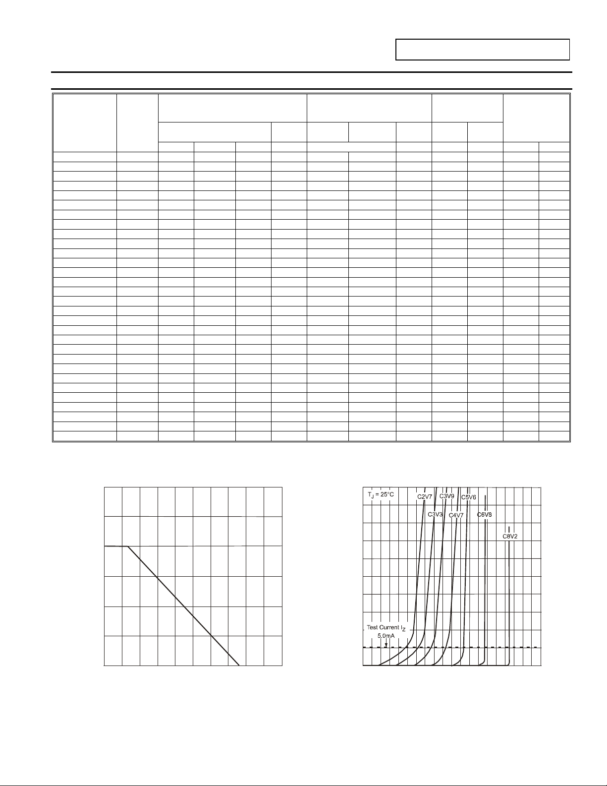
100
200
(mA)
E
30
20
Z
I, ZE
10
0
01 2 3 4 5 6
Fig. 2 Typical Zener Brea k down Characteri s t ics
V , ZENER VOLTAGE (V)
Z
891
7
0
BZX84C2V4W - BZX84C39W
Document number: DS30066 Rev. 15 - 2
2 of 4
www.diodes.com
May 2008
© Diodes Incorporated
Page 3

W
R CUR
R
T
30
20
(mA)
1,000
BZX84C2V4W - BZX84C39
V = 1V
R
V = 2V
R
EN
100
V = 1V
R
10
Z
I, ZENE
0
0
Fig. 3 Typical Zener Breakdown Characteristics
10 20 30 40
V , ZENER VOLTAGE (V)
Z
T
C , TOTAL CAPACITANCE (pF)
V = 2V
R
10
1
V , NOMINAL ZENER VOLTAGE (V)
Z
10
Fig. 4 Typical Total Capacitance vs. Nominal Zener Voltage
Ordering Information (Notes 2 & 7)
Part Number Case Packaging
(Type Number)-7-F* SOT-323 3000/Tape & Reel
* Add “-7-F” to the appropriate type number in Electrical Characteristics Table on Page 2 example: 6.2V Zener = BZX84C6V2W-7-F.
Notes: 7. For packaging details, go to our website at http://www.diodes.com/datasheets/ap02007.pdf.
T = 25 °C
J
100
Marking Information
xxx
xxx = Product Type Marking Code
(See Electrical Characteristics Table)
YM = Date Code Marking
YM
Y = Year (ex: N = 2002)
M = Month (ex: 9 = September)
Date Code Key
Year 1998 1999 2000 2001 2002 2003 2004 2005 2006 2007 2008 2009 2010 2011 2012
Code J K L M N P R S T U V W X Y Z
Month Jan Feb Mar Apr May Jun Jul Aug Sep Oct Nov Dec
Code 1 2 3 4 5 6 7 8 9 O N D
Package Outline Dimensions
K
J
A
TOP VIEW
G
H
D
SOT-323
Dim Min Max
A 0.25 0.40
C
B
B 1.15 1.35
C 2.00 2.20
D 0.65 Nominal
F 0.30 0.40
G 1.20 1.40
H 1.80 2.20
M
J 0.0 0.10
K 0.90 1.00
L 0.25 0.40
L
F
M 0.10 0.18
α
0° 8°
All Dimensions in mm
BZX84C2V4W - BZX84C39W
Document number: DS30066 Rev. 15 - 2
3 of 4
www.diodes.com
May 2008
© Diodes Incorporated
Page 4

W
BZX84C2V4W - BZX84C39
Suggested Pad Layout
Diodes Incorporated and its subsidiaries reserve the right to make modifications, enhancements, improvements, corrections or other changes
without further notice to any product herein. Diodes Incorporated does not assume any liability arising out of the application or use of any product
described herein; neither does it convey any license under its patent rights, nor the rights of others. The user of products in such applications shall
assume all risks of such use and will agree to hold Diodes Incorporated and all the companies whose products are represented on our website,
harmless against all damages.
Diodes Incorporated products are not authorized for use as critical components in life support devices or systems without the expressed written
approval of the President of Diodes Incorporated.
Y
Z
C
Dimensions Value (in mm)
Z 2.8
X 0.7
Y 0.9
C 1.9
E 1.0
X E
IMPORTANT NOTICE
LIFE SUPPORT
BZX84C2V4W - BZX84C39W
Document number: DS30066 Rev. 15 - 2
4 of 4
www.diodes.com
May 2008
© Diodes Incorporated
 Loading...