Diodes BCV47 User Manual

A
f
Product Line o
Diodes Incorporated
Features
• BV
• Darlington Transistor h
• I
• Complementary Darlington PNP Type: BCV46
• Totally Lead-Free & Fully RoHS compliant (Notes 1 & 2)
• Halogen and Antimony Free. “Green” Device (Note 3)
• Qualified to AEC-Q101 Standards for High Reliability
• PPAP capable (Note 4)
> 60V
CEO
= 500mA high Continuous Collector Current
C
> 10k @ 100mA for high gain
FE
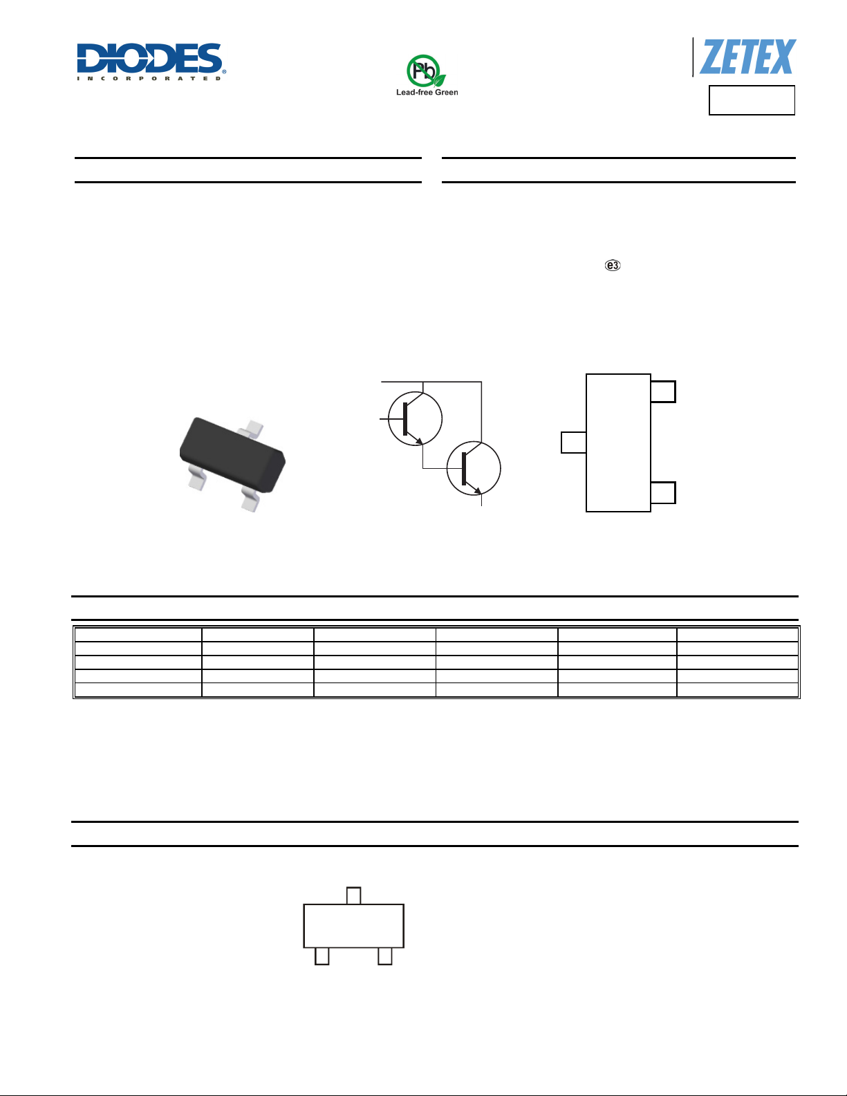
SOT23
Top View Device Symbol
C
B
60V NPN DARLINGTON TRANSISTOR IN SOT23
Mechanical Data
• Case: SOT23
• Case Material: molded plastic, “Green” molding compound
• UL Flammability Classification Rating 94V-0
• Moisture Sensitivity: Level 1 per J-STD-020
• Terminals: Finish – Matte Tin Plated Leads, Solderable per
MIL-STD-202, Method 208
• Weight 0.008 grams (approximate)
E
C
E
Top View
Pin-Out
B
BCV47
Ordering Information (Notes 4 & 5)
Part Number Compliance Marking Reel size (inches) Tape width (mm) Quantity per reel
BCV47TA AEC-Q101 ZFG 7 8 3,000
BCV47TC AEC-Q101 ZFG 13 8 10,000
BCV47QTA Automotive ZFG 7 8 3,000
BCV47QTC Automotive ZFG 13 8 10,000
Notes: 1. No purposely added lead. Fully EU Directive 2002/95/EC (RoHS) & 2011/65/EU (RoHS 2) compliant.
2. See http://www.diodes.com for more information about Diodes Incorporated’s definitions of Halogen- and Antimony-free, "Green" and Lead-free.
3. Halogen- and Antimony-free "Green” products are defined as those which contain <900ppm bromine, <900ppm chlorine (<1500ppm total Br + Cl) and
<1000ppm antimony compounds.
4. Automotive products are AEC-Q101 qualified and are PPAP capable. Automotive, AEC-Q101 and standard products are electrically and thermally
the same, except where specified.
5. For packaging details, go to our website at http://www.diodes.com.
Marking Information
ZFG
BCV47
Document number: DS33001 Rev. 4 - 2
ZFG = Product Type Marking Code
1 of 5
www.diodes.com
December 2012
© Diodes Incorporated

A
f
Product Line o
Diodes Incorporated
Maximum Ratings (@T
Collector-Base Voltage
Collector-Emitter Voltage
Emitter-Base Voltage
Continuous Collector Current
Peak Pulse Current
Base Current
Thermal Characteristics (@T
Power Dissipation
Thermal Resistance, Junction to Ambient
Thermal Resistance, Junction to Leads (Note 8)
Operating and Storage Temperature Range
Notes: 6. For the device mounted on minimum recommended pad layout FR4 PCB with high coverage of single sided 1oz copper in still air condition; the device is
measured when operating in a steady-state condition.
7. Same as note (6), except the device is mounted on 15mm x 15mm FR4 PCB.
8. Thermal resistance from junction to solder-point (at the end of the leads).
= +25°C, unless otherwise specified.)
A
Characteristic Symbol Value Unit
V
CBO
V
CEO
V
EBO
I
C
I
CM
I
B
= +25°C, unless otherwise specified.)
A
Characteristic Symbol Value Unit
(Note 6)
(Note 7) 350
(Note 6)
(Note 7) 357
R
R
T
J,TSTG
P
θJA
θJL
D
80 V
60 V
10 V
500 mA
800 mA
100 mA
310
403
350
-55 to +150
BCV47
mW
°C/W
°C/W
°C
0.4
0.3
0.2
0.1
0.0
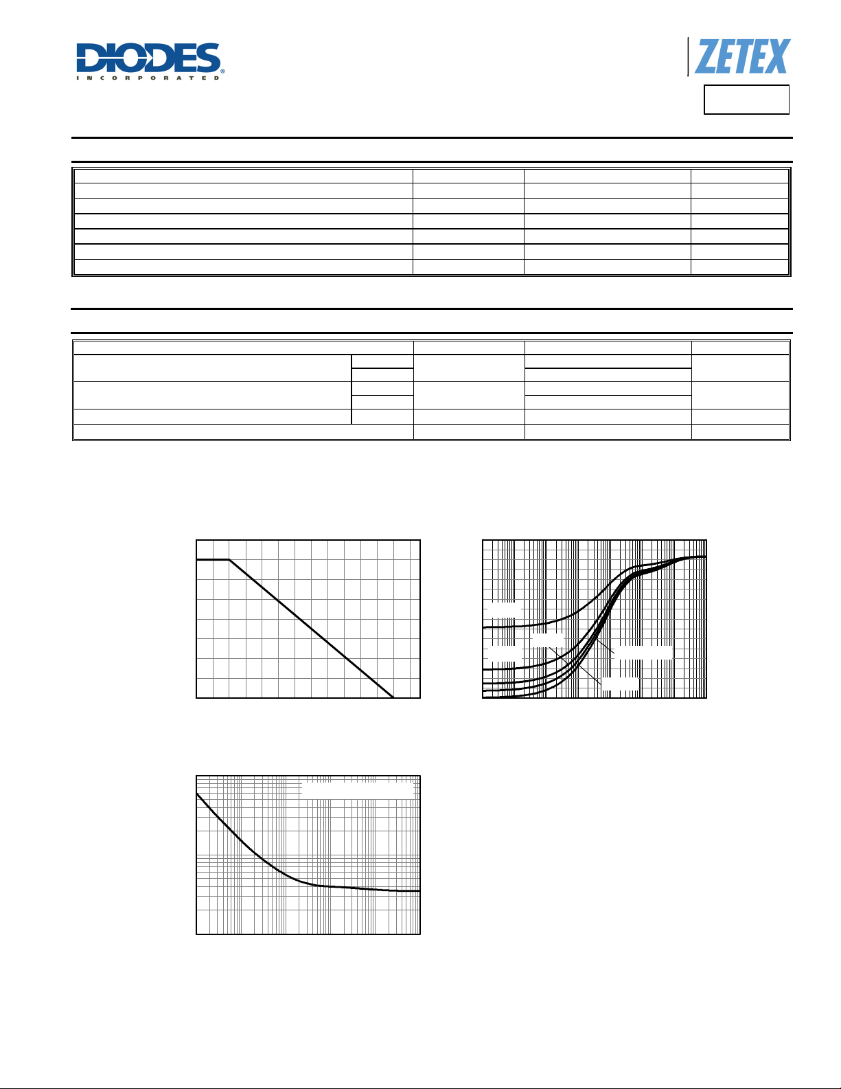
0 255075100125150
Max Power Dissipation (W)
Temperature (°C)
Derating Curve
10
Singl e Puls e. T
1
0.1
10m 100m 1 10 100 1k
Max Power Dissipation (W)
Pulse Width (s)
Pulse Power Dissipation
amb
=25°C
400
350
300
250
D=0.5
200
150
D=0.2
100
50
0
100µ 1m 10m 100m 1 10 100 1k
Thermal Resistance (°C/W)
D=0.1
Single Pulse
D=0.05
Pulse Width (s)
Transient Thermal Impedance
BCV47
Document number: DS33001 Rev. 4 - 2
2 of 5
www.diodes.com
December 2012
© Diodes Incorporated
 Loading...