Diodes BC857BLP User Manual

y
Features
• Epitaxial Die Construction
• Complementary NPN Type Available (BC847BLP)
• Ultra-Small Leadless Surface Mount Package
• “Lead Free”, RoHS Compliant (Note 1)
• Halogen and Antimony Free "Green" Device (Note 2)
• Qualified to AEC-Q101 Standards for High Reliability
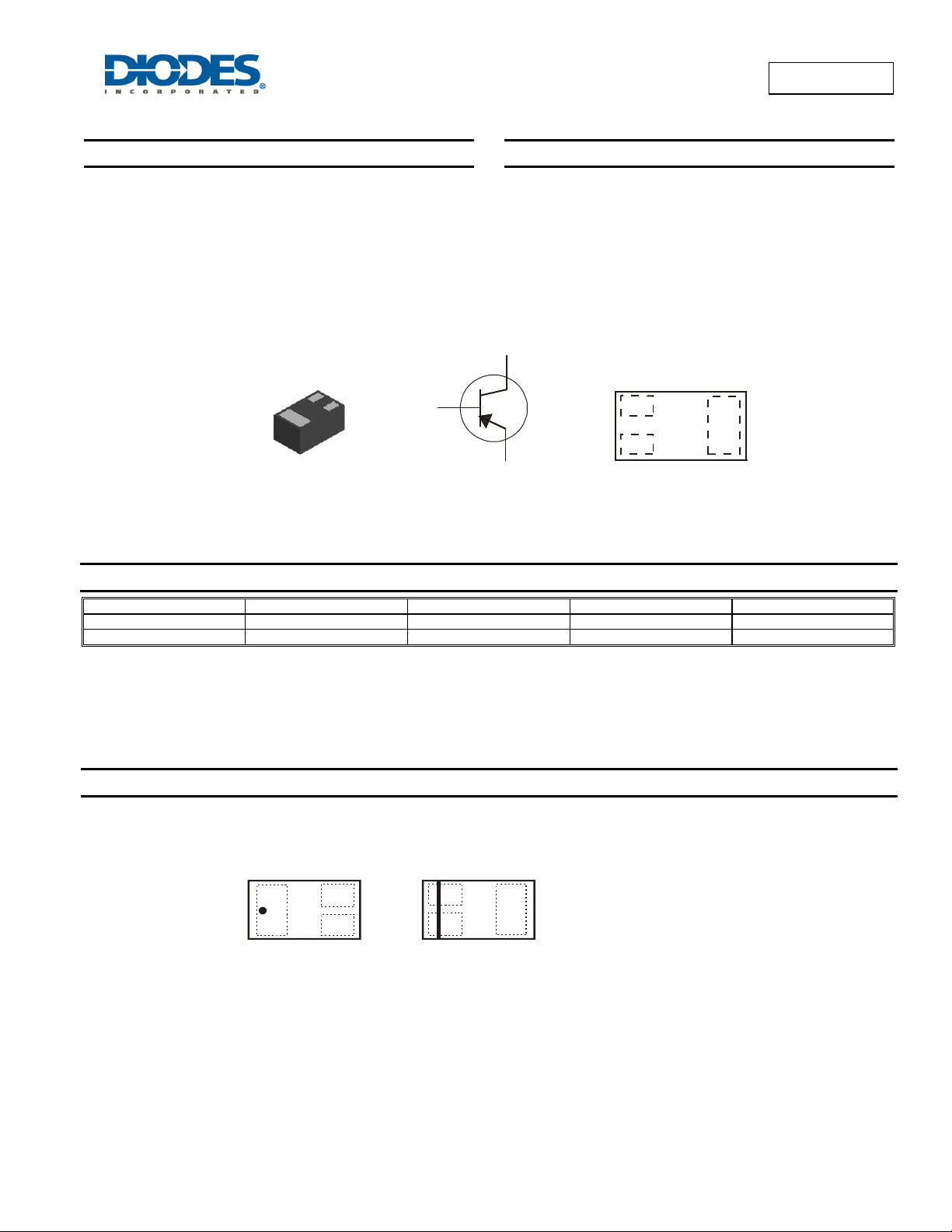
DFN1006-3
Bottom View Device S
BC857BLP
50V PNP SMALL SIGNAL SURFACE MOUNT TRANSISTOR
Mechanical Data
• Case: DFN1006-3
• Case Material: Molded Plastic, "Green" Molding Compound. UL
Flammability Classification Rating 94V-0
• Moisture Sensitivity: Level 1 per J-STD-020
• Terminals: Finish ⎯ NiPdAu over Copper leadframe. Solderable
per MIL-STD-202, Method 208
• Weight: 0.0009 grams
C
B
E
mbol
B
C
E
Top View
Pin-Out
Ordering Information (Note 3)
Product Marking Reel size (inches) Tape width (mm) Quantity per reel
BC857BLP-7 3W 7 8mm 3,000
BC857BLP-7B 3W 7 8mm 10,000
Notes: 1. No purposefully added lead.
2. Halogen and Antimony Free. Diodes Inc's "Green" policy can be found on our website at http://www.diodes.com.
3. For packaging details, go to our website at http://www.diodes.com.
Marking Information
BC857BLP
Document number: DS30526 Rev. 10 - 2
BC857BLP-7 BC857BLP-7B
3W3W
Top View
Dot Denotes
Collector Side
Top View
Bar Denotes Base
and Emitter Side
1 of 4
www.diodes.com
3W = Product Type Marking Code
February 2011
© Diodes Incorporated

θ
P, P
O
R
P
T
O
Maximum Ratings @T
= 25°C unless otherwise specified
A
Characteristic Symbol Value Unit
Collector-Base Voltage
Collector-Emitter Voltage
Emitter-Base Voltage
Collector Current
V
CBO
V
CEO
V
EBO
I
C
-50 V
-45 V
-5.0 V
-100 mA
Thermal Characteristics
Characteristic Symbol Value Unit
Power Dissipation (Note 4) @TA = 25°C PD
Thermal Resistance, Junction to Ambient Air (Note 4) @TA = 25°C
Operating and Storage Temperature Range
R
TJ, T
JA
STG
Electrical Characteristics @T
= 25°C unless otherwise specified
A
Characteristic (Note 5) Symbol Min Typ Max Unit Test Condition
Collector-Base Breakdown Voltage
Collector-Emitter Breakdown Voltage
Emitter-Base Breakdown Voltage
DC Current Gain
Collector-Emitter Saturation Voltage
Base-Emitter Saturation Voltage
Base-Emitter Voltage
Collector-Cutoff Current
Gain Bandwidth Product
Collector-Base Capacitance
Notes: 4. Device mounted on FR-4 PCB, Diodes Inc. suggested pad layout document can be found on our website at http://www.diodes.com.
5. Short duration pulse test used to minimize self-heating effect.
BV
CBO
BV
CEO
BV
EBO
hFE
V
CE(sat)
V
BE(sat)
V
BE(on)
I
CBO
fT
C
CBO
-50 — — V
-45 — — V
-5 — — V
220 260 475 —
—
—
—
-600 — -670
—
—
-90
-250
-700
-850 — —
-710
—
—
100 — — MHz
— 3.0 — pF
300
250 mW
500
-55 to +150
IC = 10μA, IB = 0
IC = 10mA, IB = 0
IE = 1μA, IC = 0
VCE = -5.0V, IC = -2.0mA
-300
-650
-750
-820
-15
-4.0
IC = -10mA, IB = -0.5mA
mV
IC = -100mA, IB = -5.0mA
IC = -10mA, IB = -0.5mA
mV
IC = -100mA, IB = -5.0mA
VCE = -5.0V, IC = -2.0mA
mV
VCE = -5.0V, IC = -10mA
VCB = -30V
nA
µA
VCB = -30V, TA = 150°C
VCE = -5.0V, IC = -10mA,
f = 100MHz
VCB = -10V, f = 1.0MHz
BC857BLP
°C/W
°C
250
N (mW)
200
I
A
150
DISSI
100
WE
D
50
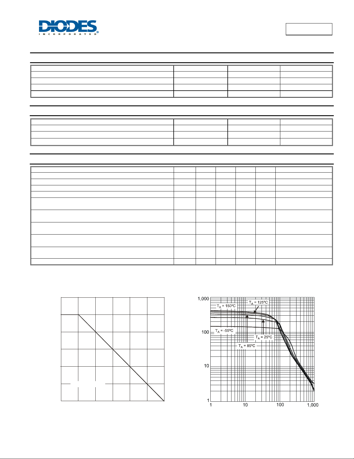
R = 500 C/W
°
θ
JA
FE
h , DC CURRENT GAIN
0
0 255075100125150
T , AMBIENT TEMPERATURE (°C)
A
Fig. 1 Power Dissipation
vs. Ambient Temperature (Note 4)
Fig. 2
I , COLLECTOR CURRENT (mA)
C
Typical DC Current Gain vs. Collector Current
BC857BLP
Document number: DS30526 Rev. 10 - 2
2 of 4
www.diodes.com
February 2011
© Diodes Incorporated
 Loading...