Diodes BC847BFA User Manual

Features
BV
I
P
0.48mm
0.4mm height package minimizing off-board profile
Complementary PNP Type BC857BFA
Totally Lead-Free & Fully RoHS compliant (Notes 1 & 2)
Halogen and Antimony Free. “Green” Device (Note 3)
Qualified to AEC-Q101 Standards for High Reliability
> 45V
CEO
= 100mA high Collector Current
C
= 435mW Power Dissipation
D
2
package footprint, 16 times smaller than SOT23
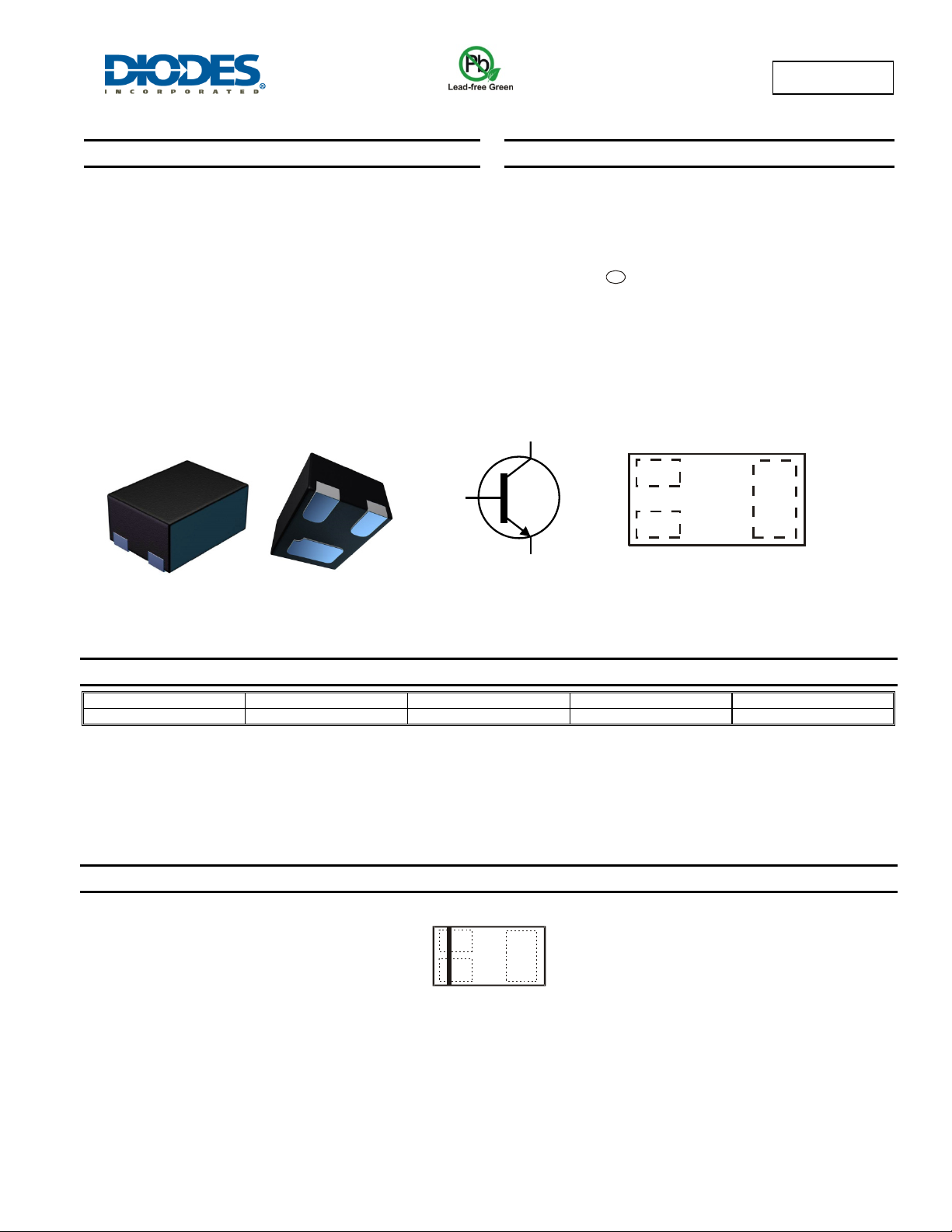
X2-DFN0806-3
Top View
Bottom View
Mechanical Data
Case: X2-DFN0806-3
Case Material: Molded Plastic, “Green” Molding Compound.
Moisture Sensitivity: Level 1 per J-STD-020
Terminals: Finish NiPdAu, Solderable per MIL-STD-202,
Weight: 0.0008 grams (approximate)
B
Device Symbol
BC847BFA
45V NPN SMALL SIGNAL TRANSISTOR IN DFN0806
UL Flammability Classification Rating 94V-0
Method 208
e4
C
B
C
E
E
Top View
Device Schematic
Ordering Information (Note 4)
Product Marking Reel size (inches) Tape width (mm) Quantity per reel
BC847BFA-7B 1F 7 8mm 10,000
Notes: 1. No purposely added lead. Fully EU Directive 2002/95/EC (RoHS) & 2011/65/EU (RoHS 2) compliant.
2. See http://www.diodes.com/quality/lead_free.html for more information about Diodes Incorporated’s definitions of Halogen- and Antimony-free, "Green"
and Lead-free.
3. Halogen- and Antimony-free "Green” products are defined as those which contain <900ppm bromine, <900ppm chlorine (<1500ppm total Br + Cl) and
<1000ppm antimony compounds.
4. For packaging details, go to our website at http://www.diodes.com/products/packages.html.
Marking Information
1F
Top View
Bar Denotes Base
and Emitter Side
1F = Product Type Marking Code
BC847BFA
Document number: DS36019 Rev. 1 - 2
1 of 6
www.diodes.com
July 2013
© Diodes Incorporated

BC847BFA
Absolute Maximum Ratings (@T
= +25°C, unless otherwise specified.)
A
Characteristic Symbol Value Unit
Collector-Base Voltage
Collector-Emitter Voltage
Emitter-Base Voltage
Continuous Collector Current
Peak Pulse Collector Current
V
CBO
V
CEO
V
EBO
I
C
I
CM
50 V
45 V
6.0 V
100 mA
200 mA
Thermal Characteristics (@T
= +25°C, unless otherwise specified.)
A
Characteristic Symbol Value Unit
Power Dissipation (Note 5)
Thermal Resistance, Junction to Ambient (Note 5)
Thermal Resistance, Junction to Lead (Note 6)
Operating and Storage and Temperature Range
P
D
R
θJA
R
θJL
T
, T
J
STG
435 mW
287
150
-55 to +150
ESD Ratings (Note 7)
C/W
C/W
C
Characteristic Symbol Value Unit JEDEC Class
Electrostatic Discharge - Human Body Model ESD HBM 4,000 V 3A
Electrostatic Discharge - Machine Model ESD MM 200 V B
Notes: 5. For the device mounted on minimum recommended pad layout 1oz copper that is on a single-sided 1.6mm FR4 PCB; device is measured under still air
conditions whilst operating in steady state condition. The entire exposed collector pad is attached to the heatsink.
6. Thermal resistance from junction to solder-point (on the exposed collector pad).
7. Refer to JEDEC specification JESD22-A114 and JESD22-A115.
Thermal Characteristics and Derating Information
V
CE(sat)
Limited
100m
DC
1s
100ms
10ms
1ms
Single Pulse
10m
T
=25°C
Collector Current (A)
C
I
amb
10m 100m 1 10
VCE Collector-Emitter Voltage (V)
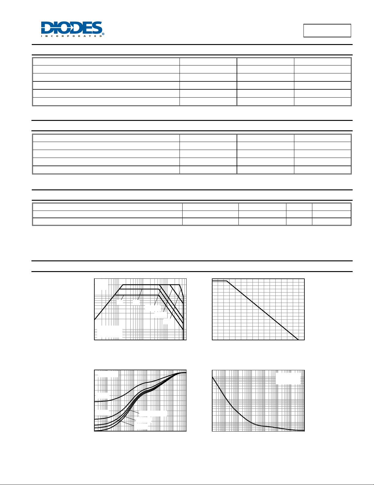
Safe Operating Area
300
T
275
250
225
200
175
150
125
100
Thermal Resistance (°C/W)
=25°C
amb
D=0.5
D=0.2
75
50
25
0
100µ 1m 10m 100m 1 10 100 1k
Single Pulse
D=0.05
D=0.1
Pulse Width (s)
Transient Thermal Impedance
0.45
0.40
0.35
0.30
0.25
0.20
0.15
0.10
0.05
0.00
0 20 40 60 80 100 120 140 160
Max Power Dissip ation (W)
Temperature (°C)
Derating Curve
100
10
1
Maximum Power (W)
100µ 1m 10m 100m 1 10 100 1k
Pulse Width (s)
Single Pulse
T
amb
Pulse Power Dissipation
=25°C
BC847BFA
Document number: DS36019 Rev. 1 - 2
2 of 6
www.diodes.com
July 2013
© Diodes Incorporated
 Loading...