

Page 1
Features
• Low Collector-Emitter Saturation Voltage, V
• Ultra-Small Leadless Surface Mount Package
• Totally Lead-Free & Fully RoHS Compliant (Note 1 & 2)
• Halogen and Antimony Free. “Green” Device (Note 3)
• Qualified to AEC-Q101 Standards for High Reliability
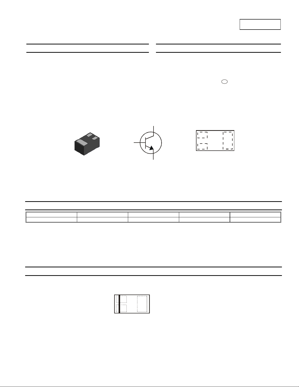
X2-DFN1006-3
Bottom View
CE(sat)
BC846BLP4
65V NPN SMALL SIGNAL SURFACE MOUNT TRANSISTOR
Mechanical Data
• Case: X2-DFN1006-3
• Case Material: Molded Plastic, "Green" Molding Compound.
UL Flammability Classification Rating 94V-0
• Moisture Sensitivity: Level 1 per J-STD-020
B
Device Symbol
• Terminals: Finish ⎯ NiPdAu over Copper leadframe. Solderable
per MIL-STD-202, Method 208
• Weight: 0.0009 grams (Approximate)
C
B
E
E
Device Schematic
e4
C
Top View
Ordering Information (Note 4)
Part Number Marking Reel size (inches) Tape width (mm) Quantity per reel
BC846BLP4-7B 3S 7 8 10,000
Notes: 1. No purposely added lead. Fully EU Directive 2002/95/EC (RoHS) & 2011/65/EU (RoHS 2) compliant.
4. For packaging details, go to our website at http://www.diodes.com.
2. See http://www.diodes.com for more information about Diodes Incorporated’s definitions of Halogen and Antimony free, "Green" and Lead-Free.
3. Halogen and Antimony free "Green” products are defined as those which contain <900ppm bromine, <900ppm chlorine (<1500ppm total Br + Cl) and
<1000ppm antimony compounds.
Marking Information
BC846BLP4
Document number: DS35751 Rev. 2 - 2
3S
Top View
Bar Denotes Base
and Emitter Side
www.diodes.com
3S = Product Type Marking Code
1 of 7
July 2012
© Diodes Incorporated
Page 2
θ
Maximum Ratings (@T
= +25°C, unless otherwise specified.)
A
Characteristic Symbol Value Unit
Collector-Base Voltage
Collector-Emitter Voltage
Emitter-Base Voltage
Collector Current - Continuous
Peak Collector Current
Peak Emitter Current
Thermal Characteristics
Characteristic Symbol Value Unit
Power Dissipation
Thermal Resistance, Junction to Ambient
Thermal Resistance, Junction to Leads (Note 7)
Operating and Storage Temperature Range
(Note 5)
(Note 6) 1
(Note 5)
(Note 6) 120
BC846BLP4
V
CBO
V
CEO
V
EBO
I
C
I
CM
I
EM
P
D
R
JA
θ
R
JL
T
, T
J
STG
80 V
65 V
6 V
100 mA
200 mA
200 mA
0.46
272
110
-55 to +150
W
°C/W
°C/W
°C
ESD Ratings (Note 8)
Electrostatic Discharge - Human Body Model ESD HBM ≥ 8,000 V 3B
Electrostatic Discharge - Machine Model ESD MM ≥ 400 V C
Notes: 5. For a device surface mounted on minimum recommended pad layout FR-4 PCB with single sided 1oz copper, in still air conditions; the device is
measured when operating in a steady-state condition. The entire exposed collector pad is attached to the heatsink.
6. Same as note 5, except device is surface mounted on 25mm X 25mm collector pad heatsink with 1oz copper.
7. Thermal resistance from junction to solder-point (at the end of the collector lead).
8. Refer to JEDEC specification JESD22-A114 and JESD22-A115.
Characteristic Symbol Value Unit JEDEC Class
BC846BLP4
Document number: DS35751 Rev. 2 - 2
2 of 7
www.diodes.com
July 2012
© Diodes Incorporated
Page 3
T
R
T T
HER
R
T
C
P, P
T
R
T P
O
R
P, P
OWER
PATIO
N
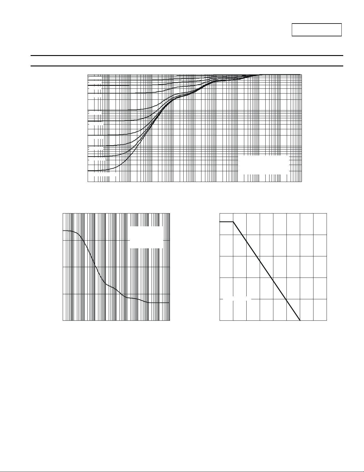
Thermal Characteristics
1
D = 0.9
D = 0.7
E
D = 0.5
AN
D = 0.3
ESIS
0.1
D = 0.1
MAL
D = 0.05
D = 0.02
0.01
D = 0.01
ANSIEN
D = 0.005
r(t),
D = Single Pulse
0.001
0.000001 0.0001 0.01 1 100 10,000
t1, PULSE DURATION TIME (sec)
Fig. 1 Transi ent Therm al Resis t ance
R (t) = r(t) * R
θθ
JA JA
R = 272°C/W
θ
JA
Duty Cycle, D = t1/ t2
BC846BLP4
1,000
(W)
100
IWE
Single Pulse
°
R = 272C/W
θ
JA
R = r * R
θθ
JA(t) (t) JA
T - T = P * R
JA JA(t)
θ
0.5
0.4
(W)
0.3
10
ANSIEN
EAK
1
(PK)
0.1
1E-06 0.0001 0.01 1 100 10,000
t1, PULSE DURATION TIME (sec)
Fig. 2 Single Pulse Maximum Power Dissipation
BC846BLP4
Document number: DS35751 Rev. 2 - 2
3 of 7
www.diodes.com
DISSI
0.2
D
R = 272C/W
0.1
0
0 50 100 150 200
°
θ
JA
T , AMBIENT TEMPERATURE (°C)
A
Fig. 3 Power Dissipation vs . Ambi ent Te m perature
July 2012
© Diodes Incorporated
Page 4

r
Electrical Characteristics (@T
= +25°C, unless otherwise specified.)
A
BC846BLP4
Characteristic Symbol Min Typ Max Unit Test Condition
OFF CHARACTERISTICS
Collector-Base Breakdown Voltage
Collector-Emitter Breakdown Voltage (Note 9)
Emitter-Base Breakdown Voltage
Collector Cutoff Current
Collector Cutoff Current
BV
BV
BV
I
CES
I
CBO
CBO
CEO
EBO
80
65
6
⎯ ⎯
⎯ ⎯
⎯ ⎯
⎯ ⎯
⎯ ⎯
V
IC = 100µA, IE = 0
V
IC = 10mA, IB = 0
V
IE = 100µA, IC = 0
15 nA
15
5.0
nA
µA
V
V
V
= 65V
CE
= 40V
CB
= 30V, TA = +150°C
CB
ON CHARACTERISTICS (Note 9)
DC Current Gain
Collector-Emitter Saturation Voltage
Base-Emitter Saturation Voltage
Base-Emitter Voltage
h
V
CE(sat)
V
BE(sat)
V
BE(on)
FE
200 270 450
⎯
⎯
580 ⎯ 650
90
220
720
870
⎯
250
600
900
⎯
700
770
⎯ V
I
C
mV
I
C
I
C
mV
I
C
V
mV
V
= 5V, IC = 2.0mA
CE
= 10mA, IB = 0.5mA
= 100mA, IB = 5.0mA
= 10mA, IB = 0.5mA
= 100mA, IB = 5.0mA
= 5V, IC = 2.0mA
CE
= 5V, IC = 10mA
CE
SMALL SIGNAL CHARACTERISTICS (Note 9)
Input Capacitance
Output Capacitance
Current Gain-Bandwidth Product
C
ibo
C
obo
f
T
Noise Figure NF
Delay time
Rise time
Storage time
Fall time
Note: 9. Measured under pulsed conditions. Pulse width ≤ 300µs. Duty cycle ≤ 2%.
t
⎯
d
t
t
s
t
f
BC846BLP4
Document number: DS35751 Rev. 2 - 2
⎯
⎯
100 300
⎯
⎯
⎯
⎯
4 of 7
www.diodes.com
6.7
1.76
⎯
⎯
⎯
2 10 dB
11.2
59.7
190.8
108.6
⎯
⎯
⎯
⎯
pF
VCB = 5V, f = 1.0MHz
pF
VCB = 10V, f = 1.0MHz
MHz
VCE = 5V, IC = 10mA, f = 100MHz
= 5V, IC = 200µA, RS = 2.0kΩ,
V
CE
f = 1.0kHz, Δf = 200Hz
ns
ns
ns
ns
= 30V,
V
CC
I
= 150mA,
C
= IB2 = 15mA
I
B1
July 2012
© Diodes Incorporated
Page 5

Typical Electrical Characteristics
500
150°C
400
300
200
, DC Current Gain
100
FE
h
85°C
25°C
-55°C
0
0.01 0.1 1 10 100 1000
125°C
IC Collector Curren t (mA)
hFE v I
C
BC846BLP4
TA = 25°C
0.3
0.2
0.1
0.0
Collector Current (A)
C
I
0.0 20.0 40.0 60.0
VCE , Collector to emitter voltage (V)
IB=4mA
IB=3mA
VCE v I
IB=2mA
C
IB=5mA
IB=1mA
IC/IB=20
-55°C
0.1
25°C
(V)
CE(SAT)
V
0.01
0.01 0.1 1 10 100
150°C
125°C
85°C
IC Collector Curren t (mA)
V
CE(SA T)
1.2
1.0
0.8
(V)
0.6
0.4
BE(SAT)
IC/IB=20
-55°C
25°C
v I
C
V
0.2
150°C
0.0
0.01 0.1 1 10 100 1000
125°C
85°C
IC Collector Curren t (mA)
V
BE(SAT)
v I
C
1.2
VCE=5V
1.0
0.8
(V)
0.6
0.4
BE(ON)
-55°C
25°C
V
0.2
0.0
0.01 0.1 1 10 100 1000
85°C
125°C
IC Collector Current (mA)
100
10
V
V
=65V
CBO
BE(ON)
v I
C
(nA)
1
CBO
I
0.1
-60 -30 0 30 60 90 120 150
TA, Ambient Temperature
I
v I
CBO
C
150°C
BC846BLP4
Document number: DS35751 Rev. 2 - 2
5 of 7
www.diodes.com
July 2012
© Diodes Incorporated
Page 6

100
C
10
ibo
1
, Total Capacitance(pF)
T
0.1
C
0.1 1 10 100
VR,Reverse Voltage (V)
VR V CT
Package Outline Dimensions
Suggested Pad Layout
BC846BLP4
Document number: DS35751 Rev. 2 - 2
A
A1
D
b2
E
L2
X
1
X
G2
Y
Z
BC846BLP4
1000
f = 1MHz
C
obo
b1
e
L1L3
C
G1
6 of 7
www.diodes.com
100
f =100MHz
Vce=5V
10
110100
, Gain Bandwidth Product (MHz)
T
f
IC, Collector Curre nt (mA)
IC V f
X2-DFN1006-3
Dim Min Max Typ
A
⎯
A1 0 0.05 0.03
b1 0.10 0.20 0.15
b2 0.45 0.55 0.50
D 0.95 1.05 1.00
E 0.55 0.65 0.60
e
⎯ ⎯
L1 0.20 0.30 0.25
L2 0.20 0.30 0.25
L3
⎯ ⎯
All Dimensions in mm
Dimensions Value (in mm)
Z 1.1
G1 0.3
G2 0.2
X 0.7
X1 0.25
Y 0.4
C 0.7
0.40
T
⎯
0.35
0.40
July 2012
© Diodes Incorporated
Page 7

IMPORTANT NOTICE
DIODES INCORPORATED MAKES NO WARRANTY OF ANY KIND, EXPRESS OR IMPLIED, WITH REGARDS TO THIS DOCUMENT,
INCLUDING, BUT NOT LIMITED TO, THE IMPLIED WARRANTIES OF MERCHANTABILITY AND FITNESS FOR A PARTICULAR PURPOSE
(AND THEIR EQUIVALENTS UNDER THE LAWS OF ANY JURISDICTION).
Diodes Incorporated and its subsidiaries reserve the right to make modifications, enhancements, improvements, corrections or ot her changes
without further notice to this document and any product described herein. Diodes Incorporated does not assume any liability arising out of the
application or use of this document or any product described herein; neither does Diodes Incorporated convey any license under its patent or
trademark rights, nor the rights of others. Any Customer or user of this document or products described herein in such applications shall assume
all risks of such use and will agree to hold Diodes Incorporated and all the companies whose products are represented on Diodes Incorporated
website, harmless against all damages.
Diodes Incorporated does not warrant or accept any liability whatsoever in respect of any products purchased through unauthorized sales channel.
Should Customers purchase or use Diodes Incorporated products for any unintended or una uthorized appli cation, Customers shall indemnif y and
hold Diodes Incorporated and its representatives harmless against all claims, damages, expenses, and attorney fees arising out of, directly or
indirectly, any claim of personal injury or death associated with such unintended or unauthorized application.
Products described herein may be covered by one or more United States, international or foreign patents pending. Product names and markings
noted herein may also be covered by one or more United States, international or foreign trademarks.
LIFE SUPPORT
Diodes Incorporated products are specifically not authorized for use as critical components in life support devices or systems without the express
written approval of the Chief Executive Officer of Diodes Incorporated. As used herein:
A. Life support devices or systems are devices or systems which:
1. are intended to implant into the body, or
2. support or sustain life and whose failure to perform when properly used in accordance with instructions for use provided in the
labeling can be reasonably expected to result in significant injury to the user.
B. A critical component is any component in a life support device or system whose failure to perform can be reasonably expected to cause the
failure of the life support device or to affect its safety or effectiveness.
Customers represent that they have all necessary expertise in the safety and regulatory ramifications of their life support devices or systems, and
acknowledge and agree that they are solely responsible for all legal, regulatory and safety-related requirements concerni ng the ir pro ducts and an y
use of Diodes Incorporated products in such safety-critical, life support devices or systems, notwithstanding any devices- or systems-related
information or support that may be provided by Diodes Incorporated. Further, Customers must fully indemnify Diodes Incorporated and its
representatives against any damages arising out of the use of Diodes Incorporated products in such safety-critical, life support devices or systems.
Copyright © 2012, Diodes Incorporated
www.diodes.com
BC846BLP4
BC846BLP4
Document number: DS35751 Rev. 2 - 2
7 of 7
www.diodes.com
July 2012
© Diodes Incorporated
 Loading...