

Page 1
A
f
A
Features
BV
BV
BV
I
Integrated Collector-Emitter Diode to act as free-wheeling diode
Anti-saturation for faster switching
Lead-Free Finish; RoHS Compliant (Notes 1 & 2)
Halogen and Antimony Free. “Green” Device (Note 3)
> 450V
CEO
> 700V
CES
> 9V
EBO
= 1.5A high Continuous Collector Current
C
Applications
Low power AC-DC SMPS for:
Battery Chargers for Mobile Phone / Tablets / Smartphones
Power Supply for DVD / STB
LED lighting
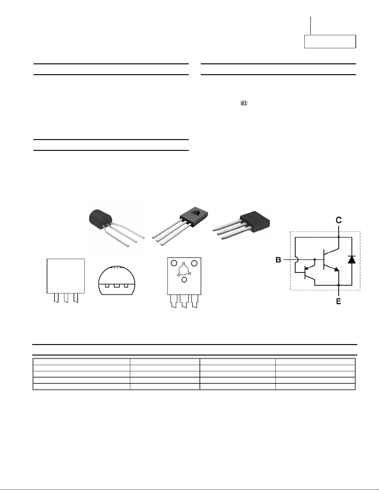
TO92
(Bulk)
Flat Face
View
B C E
Pin-Out
TO92
(Ammo)
E C B
Bottom View
TO126
Front Face View
Pin-Out
Product Line o
Green
Diodes Incorporated
PT13003D
450V NPN HIGH VOLTAGE POWER TRANSISTOR
Mechanical Data
Case: TO92, TO126 or TO251
Case Material: Molded Plastic, "Green" Molding Compound; UL
Flammability Classification Rating 94V-0
Terminals: Matte Tin Finish; Solderable per MIL-STD-202,
Method 208
Weight: TO92: 200mg (Approximate)
TO126: 400mg (Approximate)
TO251: 340mg (Approximate)
TO251
ECB
Front Face View
ECB
Pin-Out
Device Schematic
Ordering Information (Note 4)
Product Package Marking Quantity
APT13003DZ-G1 TO92 (Straight Legs) 13003DZ-G1 10,000 Bulk, Loose per Box
APT13003DZTR-G1 TO92 (Joggled Legs) 13003DZ-G1 2,000 Taped, per Ammo Box
APT13003DU-G1 TO126 GU13003D 4,000 Bulk, Loose per Box
APT13003DI-G1 TO251 APT13003DI-G1 3,600 per Box in Tubes
Notes: 1. EU Directive 2002/95/EC (RoHS) & 2011/65/EU (RoHS 2) compliant. All applicable RoHS exemptions applied.
2. See http://www.diodes.com/quality/lead_free.html for more information about Diodes Incorporated’s definitions of Halogen- and Antimony-free, "Green"
and Lead-free.
3. Halogen- and Antimony-free "Green” products are defined as those which contain <900ppm bromine, <900ppm chlorine (<1500ppm total Br + Cl) and
<1000ppm antimony compounds.
4. For packaging details, go to our website at http://www.diodes.com/products/packages.html
APT13003D
Datasheet Number: DS36347 Rev. 1 - 2
1 of 7
www.diodes.com
July 2013
© Diodes Incorporated
Page 2
A
f
A
Marking Information
Absolute Maximum Ratings (@T
Collector-Emitter Voltage (VBE = 0V) V
Collector-Emitter Voltage
Emitter-Base Voltage
Continuous Collector Current
Peak Pulse Collector Current
Continuous Base Current
Peak Pulse Base Current
TO92 TO126
13003D
Z-G1
YWW8XX
GU13003D
YWW8XX
Flat Face
View
Front Face View Front Face View
Characteristic Symbol Value Unit
TO251
APT13003D
I-G1
YWW8XX
= +25°C, unless otherwise specified.)
A
Product Line o
Diodes Incorporated
PT13003D
= Manufacturers’ code marking
For TO92, 13003DZ-G1 = Product Type Marking ID
For TO126, GU13003D = Product Type Marking ID
For TO251, APT13003DI-G1= Product Type Marking ID
YWW = Date Code Marking
8 = Assembly site code
XX = Batch Number
CES
V
CEO
V
EBO
I
C
I
CM
I
B
I
BM
e.g. 312 = Year 2013, Week 12.
0.75 A
700 V
450 V
9 V
1.5 A
3 A
1.5 A
Thermal Characteristics (@T
= +25°C, unless otherwise specified.)
A
Characteristic Symbol Value Unit
Power Dissipation
Thermal Resistance, Junction to Ambient Air
For TO92
For TO126@ TC = +25°C
P
D
For TO251@ TC = +25°C
For TO92
For TO126 96
R
θJA
1.1
20
24
113.6
W
C/W
For TO251 110
Thermal Resistance, Junction to Case
For TO92
For TO126 6.25
R
θJC
83.3
C/W
For TO251 5.0
Operating and Storage Temperature Range
T
J,TSTG
-65 to +150
C
ESD Ratings (Note 6)
Characteristic Symbol Value Unit JEDEC Class
Electrostatic Discharge - Human Body Model ESD HBM ≥ 8,000 V 3B
Electrostatic Discharge - Machine Model ESD MM ≥ 400 V C
Note: 6. Refer to JEDEC specification JESD22-A114 and JESD22-A115.
APT13003D
Datasheet Number: DS36347 Rev. 1 - 2
2 of 7
www.diodes.com
July 2013
© Diodes Incorporated
Page 3
A
f
A
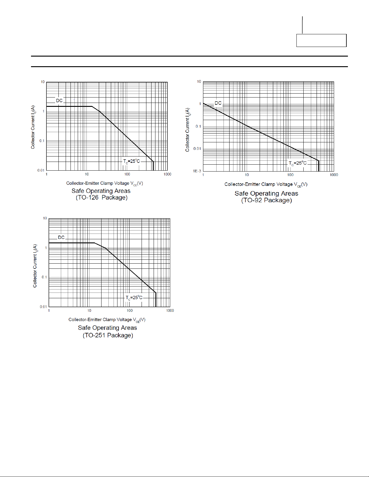
Safe Operating Areas and Derating Information (@T
Product Line o
Diodes Incorporated
= +25°C, unless otherwise specified.)
A
PT13003D
APT13003D
Datasheet Number: DS36347 Rev. 1 - 2
3 of 7
www.diodes.com
July 2013
© Diodes Incorporated
Page 4

A
f
A
Electrical Characteristics (@T
Characteristic Symbol Min Typ. Max Unit Test Condition
Collector-Emitter Breakdown Voltage
Collector-Emitter Breakdown Voltage
Emitter-Base Breakdown Voltage
Collector Cutoff Current
DC current transfer Static ratio (Note 7)
Collector-Emitter Saturation Voltage (Note 7)
Base-Emitter Saturation Voltage (Note 7)
Output Capacitance
Transition Frequency
Turn-on Time with Resistive Load
Storage Time with Resistive Load
Fall Time with Resistive Load
Note: 7. Measured under pulsed conditions. Pulse width ≤ 300μs. Duty cycle ≤2%.
= +25°C, unless otherwise specified.)
A
BV
CES
BV
CEO
BV
EBO
I
CEV
h
FE
V
CE(sat)
V
BE(sat)
C
ob
f
T
t
on
t
s
t
f
700
450
9
16
5.0
4
18
0.35
Product Line o
Diodes Incorporated
V
IC = 100µA, VBE = 0V
V
IC = 100µA
V
IE = 100µA
10 µA
30
25
0.3
0.4
1.0
1.2
0.7
3.0
V
V
pF
MHz
µs
V
= 700V, VBE = -1.5V
CE
I
= 0.5A, V
C
= 1.0A, V
I
C
= 0.5A, IB = 0.1A
I
C
I
= 1A, IB = 0.25A
C
= 0.5A, IB = 0.1A
I
C
= 1A, IB = 0.25A
I
C
V
= 10V, f = 0.1MHz
CB
= 0.1A, V
I
C
= 1A,VCC = 125V, IB1 = 0.2A,
I
C
= -0.2A
I
B2
PT13003D
= 2V
CE
= 2V
CE
= 10V
CE
Typical Electrical Characteristics (@T
= +25°C, unless otherwise specified.)
A
APT13003D
Datasheet Number: DS36347 Rev. 1 - 2
4 of 7
www.diodes.com
July 2013
© Diodes Incorporated
Page 5

A
f
A
Package Outline Dimensions
Please see AP02002 at http://www.diodes.com/datasheets/ap02002.pdf for latest version.
TO92 Type C
E
L
h
TO126
APT13003D
Datasheet Number: DS36347 Rev. 1 - 2
D
EJECTION MARK
b
1
e
e
BUL
K
D
1
A
2
ø
D
E
b
1
b
L
e
e
1
A
EJECTION MARK
E
L
2
L
1
b
e
2
e
c
A
A
2
Y
ø
L
1
2
TAPED
AMMO
h
c
5 of 7
www.diodes.com
Product Line o
Diodes Incorporated
TO92 Type C
Dim Min Max Typ
L
3
A 3.30 3.70 -
A2 1.10 1.40 -
b 0.38 0.55 -
c 0.36 0.51 -
D 4.40 4.70 -
D1 3.430 - -
E 4.30 4.70 -
e - - 1.27
e2 2.440 2.640 -
h 0.00 0.38 -
L 14.10 14.50 -
L1 12.50 14.50 -
L3 2.50 3.50 -
ø - 1.60 -
All Dimensions in mm
TO126
Dim Min Max Typ
A 2.400 2.900 -
A2 1.060 1.500 -
b 0.660 0.860 -
b1 1.170 1.470 -
c 0.400 0.600 -
D 7.400 8.200 -
E 10.60 11.20 -
e - - 2.280
e1 - - 4.560
h 0.00 0.30 -
L 14.50 15.90 -
L1 1.700 2.100 -
Y 3.600 3.900 -
ø 3.100 3.550 -
All Dimensions in mm
PT13003D
July 2013
© Diodes Incorporated
Page 6

A
f
A
Product Line o
Diodes Incorporated
PT13003D
Package Outline Dimensions (cont.)
Please see AP02002 at http://www.diodes.com/datasheets/ap02002.pdf for latest version.
TO251
Note: For high voltage applications, the appropriate industry sector guidelines should be considered with regards to voltage spacing between terminals.
E
2
E
L
D
D
2
b
e
e
1
A
A
3
Option
2
45°
TO251
Dim Min Max
A 2.200 2.400
A2 0.890 1.150
A3 0.450 0.550
Option
3
b 0.550 0.740
c 0.450 0.570
D 6.400 6.750
D2 5.200 5.400
E 5.950 6.250
E2 0.900 1.250
e 2.240 2.340
e1 4.430 4.730
c
A
2
L 8.900 9.500
All Dimensions in mm
APT13003D
Datasheet Number: DS36347 Rev. 1 - 2
6 of 7
www.diodes.com
July 2013
© Diodes Incorporated
Page 7

A
f
A
Product Line o
IMPORTANT NOTICE
DIODES INCORPORATED MAKES NO WARRANTY OF ANY KIND, EXPRESS OR IMPLIED, WITH REGARDS TO THIS DOCUMENT,
INCLUDING, BUT NOT LIMITED TO, THE IMPLIED WARRANTIES OF MERCHANTABILITY AND FITNESS FOR A PARTICULAR PURPOSE
(AND THEIR EQUIVALENTS UNDER THE LAWS OF ANY JURISDICTION).
Diodes Incorporated and its subsidiaries reserve the right to make modifications, enhancements, improvements, corrections or other changes
without further notice to this document and any product described herein. Diodes Incorporated does not assume any liability arising out of the
application or use of this document or any product described herein; neither does Diodes Incorporated convey any license under its patent or
trademark rights, nor the rights of others. Any Customer or user of this document o r products described herein in such applica tions shall assume
all risks of such use and will agree to hold Diodes Incorporated and all the companies whose products are represented on Diodes Incorporated
website, harmless against all damages.
Diodes Incorporated does not warrant or accept any liability whatsoever in respect of any products purchased through unauthorized sales channel.
Should Customers purchase or use Diodes Incorporated products for any unintended or unauthorize d application, Customers shall indemnify and
hold Diodes Incorporated and its representatives harmless against all claims, damages, expenses, and attorney fees arising out of, directly or
indirectly, any claim of personal injury or death associated with such unintended or unauthorized application.
Products described herein may be covered by one or more United States, international or foreign patents pending. Product names and markings
noted herein may also be covered by one or more United States, international or foreign trademarks.
This document is written in English but may be translated into multiple languages for reference. Onl y the English version of this document is the
final and determinative format released by Diodes Incorporated.
LIFE SUPPORT
Diodes Incorporated products are specifically not authorized for use as critical components in life support devices or systems without the express
written approval of the Chief Executive Officer of Diodes Incorporated. As used herein:
A. Life support devices or systems are devices or systems which:
1. are intended to implant into the body, or
2. support or sustain life and whose failure to perform when properly used in accordance with instructions for use provided in the
labeling can be reasonably expected to result in significant injury to the user.
B. A critical component is any component in a life support device or system whose failure to perform can be reasonably expected to cause the
failure of the life support device or to affect its safety or effectiveness.
Customers represent that they have all necessary expertise in the safety and regulatory ramifications of their life support devices or systems, and
acknowledge and agree that they are solely responsible for all legal, regulatory and safety-related requirements concerning their products and any
use of Diodes Incorporated products in such safety-critical, life support devices or systems, notwithstanding any devices- or systems-related
information or support that may be provided by Diodes Incorporated. Further, Customers must fully indemnify Diodes Incorporated and its
representatives against any damages arising out of the use of Diodes Incorporated products in such safety-critical, life support devices or systems.
Copyright © 2012, Diodes Incorporated
www.diodes.com
Diodes Incorporated
PT13003D
APT13003D
Datasheet Number: DS36347 Rev. 1 - 2
7 of 7
www.diodes.com
July 2013
© Diodes Incorporated
 Loading...