

Page 1
API9221
CAR/WALL or USB SUPPLY INPUT LITHIUM BATTERY
CHARGER with OVP USB BYPASS and 10mA LDO
Description
The API9221 has two supply inputs for highly integrated
portable applications, enabling charging from a USB host,
wall adapter, or car adapter.
The
pin indicates to a host controller that a safe and
PPR
valid supply is connected to either VUSB or VDC. The hig her
charge current option from VDC will take priority if both
supplies are connected. The host controller can control the
state of charging via the enable pin
. The API9221
EN
implements the constant current/constant voltage (CC/CV)
charge algorithm for Lithium based battery cells. The
connected cell will be charged to 4.2V with an accuracy of
1% over the entire temperature range. The termination
current is programmable via an external resistor, R
The
reached, and is reset by
pin indicates when the termination current is
CHG
EN , power off, or battery below
3.9V. The maximum charge current can be programmed
independently via the resistors R
IUSB
and R
IVDC
The API9221 comes with several protection features. To
prevent system damage, the VUSB pin uses over voltage
NEW PRODUCT
protection (OVP) at 5.4V, and the VDC OVP is at 6.9V.
Above these levels, the non-operating device is protected
against damage up to 28V. For control and system start-up
the API9221 has a current limited linear regulator.
To protect the chip against excessive power dissipation,
temperature monitoring is integrated, which folds back the
current to a safe level. As the temperature rises, this foldback begins at 125°C without completely interrupting
charging.
Applications
• Handheld Consumer Devices
• Cell Phones, PDAs, MP3 Players
• Handheld Test Equipment
• Digital Still Cameras
• Multimedia players
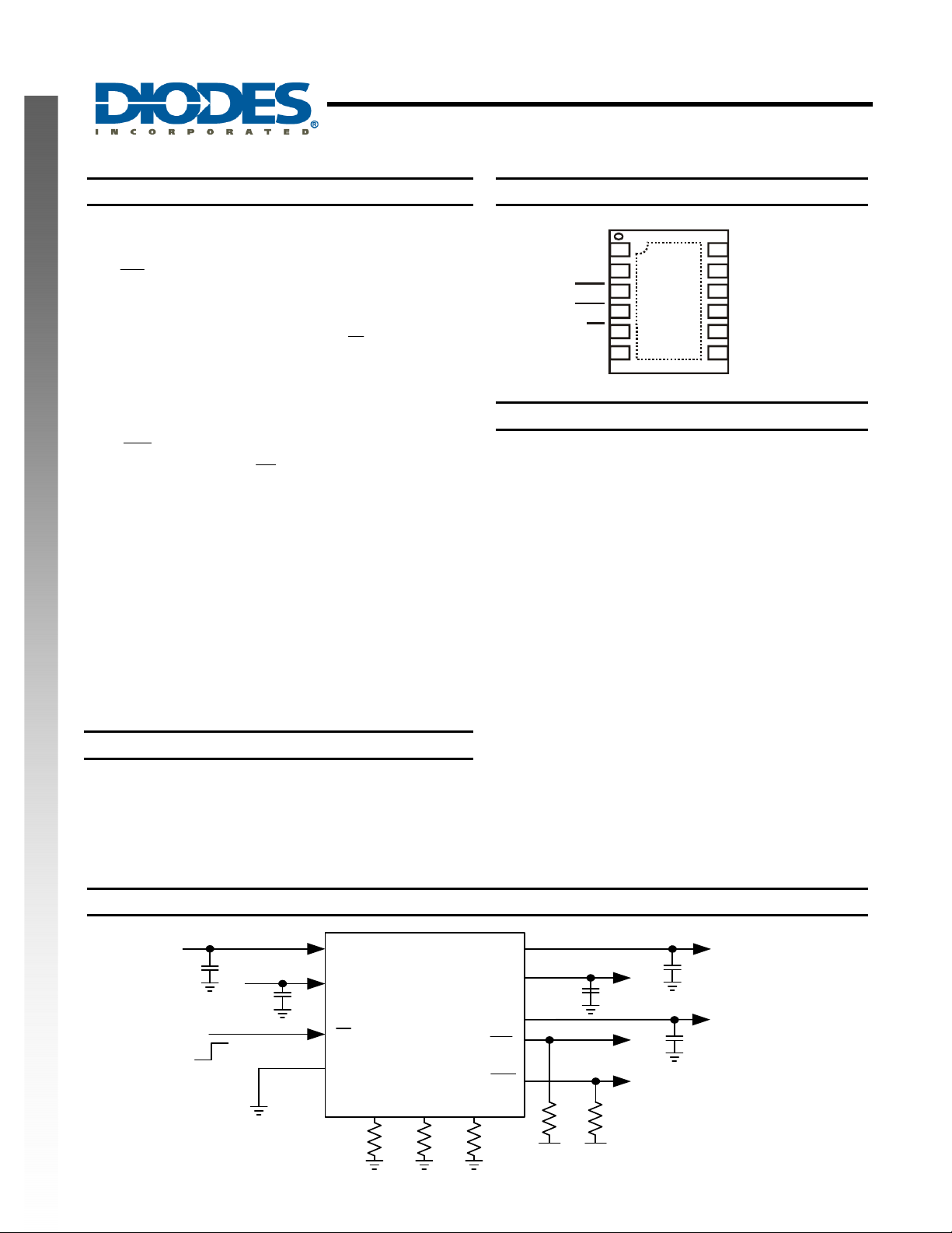
Pin Assignments
(Top View)
1
VDC
PPR
CHG
EN
IMIN
2
3
Exposed Pad
4
5
6
VUSB
U-DFN4030-12
IMIN
.
Features
• Linear Lithium Ion / Lithium Polymer charging IC
• Supplied from USB host or car/wall adapter
• Overvoltage protection USB: 5.4V, wall:6.9V
.
• Supply inputs safe up to 28V
• Fast charging with maximum current of 1.2A
• Integrated linear regulator of 4.9V at 10mA with
current limit
• Separate resistor-programmable charging
current for wall and USB
• Resistor programmable end-of-charge
• Current limit on USB bypass path
• Indicator pins for charging and power present
• Enable pin to enable host control charging
• Reverse current protection
• Thermal protection
• U-DFN4030-12: Available in “Green” Molding
Compound
(No Br, Sb)
• Lead Free Finish/ RoHS Compliant (Note 1)
Note: 1. EU Directive 2002/95/EC (RoHS). All applicable RoHS
exemptions applied. Please visit our website at
http://www.diodes.com/products/lead_free.html.
12
VDC_LDO
11
BAT
10
USB_BYP
9
IVDC
8
GND
7
IUSB
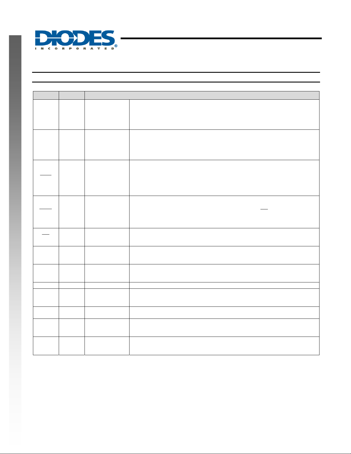
Typical Application Circuit
DC Input
USB Input
OFF
ON
API9221
Document number: DS32204 Rev. 2 - 2
VDC
VUSB
EN
GND
API9221
IMIN IUSB IVDC
IMIN
R
IUSB
R
VDC_LDO
BAT
USB_BYP
PPR
CHG
IVDC
R
1 of 15
www.diodes.com
To Battery
I/O_VDD
To MCU
I/O_VDD
LDO Output
USB_BYP
© Diodes Incorporated
November 2011
Page 2
Pin Descriptions
Name Pin # Descriptions
VDC 1
VUSB 2
PPR
NEW PRODUCT
CHG
EN
IMIN 6
IUSB 7
GND 8 Ground Ground return path.
IVDC 9
USB_BYP 10
BAT 11 Battery connector
VDC_LDO 12 LDO output
API9221
CAR/WALL or USB SUPPLY INPUT LITHIUM BATTERY
CHARGER with OVP USB BYPASS and 10mA LDO
The recommended input to this pin is 4.5V to 6.7V with a maximum safe value of
Input pin from a
wall AC/DC or car
adapter
USB Host device
input
Power present
3
signal output,
active-low
Charge indicator
4
output, active-low
Charge enable
5
input, active-low
Current setting for
end-of-charge
state
Current setting,
USB Power
Current setting,
wall or car adapter
USB Bypass
output
28V. If a sufficient voltage is detected on VDC, no charge current is taken from
the VUSB pin. Internal OVP trips at 6.9V. The input current can be programmed
with a resistor at IVDC (pin 9). Decoupling with a 1μF ceramic capacitor is
recommended.
The recommended input to this pin is 4.5V to 5.3V with a maximum safe value of
28V. Internal OVP trips at 5.4V. The supply current drawn at this pin is the sum
of the charge current and the USB_BYP current. Decoupling with a 1μF ceramic
capacitor is recommended. Special attention has to be given to the maximum
capacitance on the USB connection. Refer to the USB standard.
The power present pin can indicate to a host processor that an external source is
present and that current can be derived from the input. This is an open drain
output pin, which goes LOW when a valid source voltage is connected to either
VUSB or VDC. If connected to a processor I/O a pull up resistor should be
utilized.
Alternatively this pin can be used to drive an indicator LED up to 10mA.
Open drain pin is pulled LOW when charging is performed. Goes high when
charge current reaches IMIN. Remains high (including top-up), until the battery
EN
voltage falls below 3.9V or the device is power cycled or
connected to a processor I/O a pull up resistor should be utilized.
Alternatively this pin can be used to drive an indicator LED up to 10mA.
Logic level input pin to control charging from an external processor. An internal
600kΩ (nominally) pull-down resistor is provided, This pin normally requires a
pull up resistor when connected to a processor I/O.
The end-of-charge current is set by a resistor connected from this pin to GND.
This applies to charging from either VDC or VUSB.
The USB input maximum charging current is set by a resistor connected from this
pin to GND. This current is also limited by a thermally controlled current fold-
back circuit.
VDC input maximum charging current is set by a resistor connected from this pin
to GND. This current is also limited by a thermally controlled current fold-back
circuit.
Provides an external load path from the USB input, with current limiting. Protected
against reverse current.
Connect this pin to the positive terminal of the battery. This pin is also used to
monitor the charge state of the battery. It is not recommended to operate the part
without a battery connected to this pin. Protected against reverse current.
Low current linear regulator for system supply, available when a valid VDC input
supply is used. Stabilize with a 0.1F to 1F ceramic capacitor to ground.
Protected against reverse current.
is cycled. If
API9221
Document number: DS32204 Rev. 2 - 2
2 of 15
www.diodes.com
November 2011
© Diodes Incorporated
Page 3
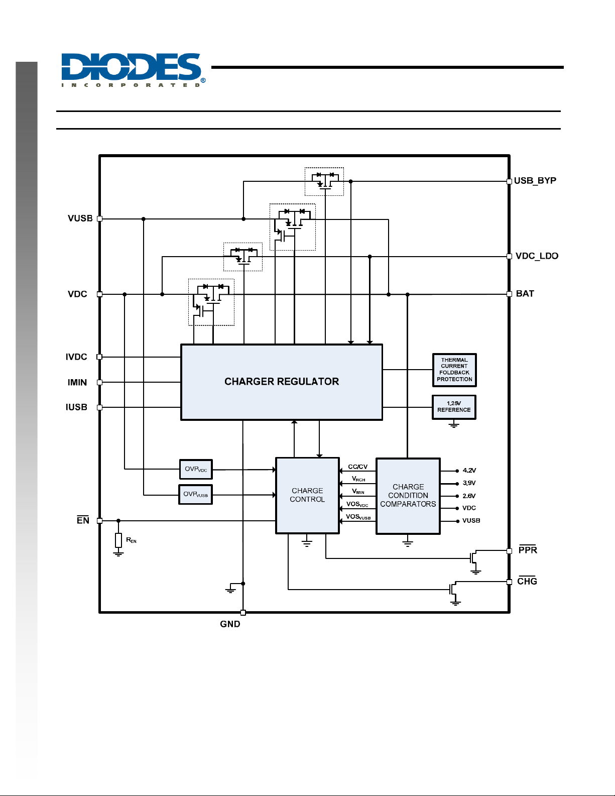
Functional Block Diagram
API9221
CAR/WALL or USB SUPPLY INPUT LITHIUM BATTERY
CHARGER with OVP USB BYPASS and 10mA LDO
NEW PRODUCT
API9221
Document number: DS32204 Rev. 2 - 2
3 of 15
www.diodes.com
November 2011
© Diodes Incorporated
Page 4
Absolute Maximum Ratings
Symbol Parameter Rating Unit
VDC, VUSB to GND -0.3 to 28V V
USB_BYP, VDC_LDO -0.3 to 7V V
ESD Susceptibility (Note 2)
HBM Human Body Model 2 kV
MM Machine Model 200 V
Thermal Resistance (Note 3)
Symbol Parameter Rating Unit
JA
NEW PRODUCT
JC
EN
CHG
Junction to Ambient 41
Junction to Case 3.5
CAR/WALL or USB SUPPLY INPUT LITHIUM BATTERY
CHARGER with OVP USB BYPASS and 10mA LDO
, IMIN, IVDC, IUSB, BAT -0.3 to 7V
,
PPR
-0.3 to 7V
API9221
V
V
°C/W
Recommended Operating Conditions (Note 4)
Symbol Parameter Rating Unit
Ambient Temperature Range -40 to +85 °C
VUSB
VDC
I
VDC_CHRG
I
USB_CHRG
I
Notes: 2. Semiconductor devices are ESD sensitive and may be damaged by exposure to ESD events. Suitable ESD precautions should be taken when
handling and transporting this device.
3. Test condition for U-DFN4030-12: Measured on approximately 1” square of 1 oz copper.
4. The device function is not guaranteed outside of the recommended operating conditions.
USB-BYP
I
LDO
Supply Voltage (VUSB) 4.5 to 5.3 V
Supply Voltage (VDC) 4.5 to 6.7 V
Typical Adapter Charge Current
Typical USB Charge Current
Typical USB Bypass Current
Typical LDO Current
0.1 to 1.2
46.5 to 465
0 to 200
0 to 10
A
mA
mA
mA
API9221
Document number: DS32204 Rev. 2 - 2
4 of 15
www.diodes.com
November 2011
© Diodes Incorporated
Page 5
CAR/WALL or USB SUPPLY INPUT LITHIUM BATTERY
CHARGER with OVP USB BYPASS and 10mA LDO
Electrical Characteristics
API9221 is tested at VDC = VUSB = 5V at an ambient temperature of +25°C unless otherwise noted.
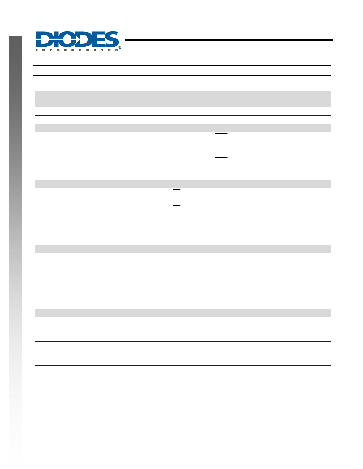
Symbol Parameter Test Conditions Min Typ. Max Unit
CHARGER POWER-ON THRESHOLDS
Rising VUSB/VDC Threshold
Falling VUSB/VDC Threshold
Rising VDC or VUSB, relative
to V
BAT
Falling VDC or VUSB, relative
to V
BAT
BAT Pin Sink Current
VDC Pin Supply Current
VUSB Pin Supply Current
VDC/VUSB Pin Supply Current
Final Output Voltage, BAT Pin
VDC Linear ON-resistance
VUSB Linear ON-resistance
VDC Pin Output Voltage
VDC Constant Current
VDC Trickle Charge Current
V
= 4.0V, use
BAT
CHG
pin to indicate the
comparator output
= 4.0V, use
V
BAT
CHG
pin to indicate the
comparator output
= HIGH or both inputs
EN
are floating
= HIGH, I
EN
= HIGH, USB_BYP
EN
LDO
= 0
disconnected
EN
= LOW, I
LDO
= 0,
USB_BYP disconnected
Load = 10mA 4.158 4.2 4.242 V
Load = 10mA
(T
= +25°C)
J
V
BAT
=3.8V, I
VDC
= 0.3A,
(TJ = +25°C)
= 3.8V, I
V
BAT
= +25°C)
(T
J
V
= 3.8V
BAT
R
= 12.4k,
IVDC
V
= 2.7V to 3.8V
BAT
= 12.4k,
R
IVDC
V
= 2.2V, given as a %
BAT
of the I
VDC_CHARGE
USB
= 0.3A,
NEW PRODUCT
VPO
R
VPO
F
INPUT VOLTAGE OFFSET
VOSHC
VOSLC
STANDBY CURRENT
I
STANDBY
I
VDC
I
VUSB
I
VDC_VUSB
VOLTAGE REGULATION
V
R
R
BATMAX
DS(ON)_VDC
DS(ON)_VUSB
CHARGE CURRENT
V
IVDC
I
VDC_CHRG
I
VDC_TRKL
API9221
3.4 3.9 4.2 V
3.2 3.7 4.0 V
- 150 250 mV
20 80 - mV
- 0.05 0.5 µA
- 380 460 µA
- 330 400 µA
- 0.63 1.1 mA
4.174 4.2 4.226 V
- 550 - m
- 550 - m
1.22 1.25 1.28 V
450 550 600 mA
15 17 19 %
API9221
Document number: DS32204 Rev. 2 - 2
5 of 15
www.diodes.com
November 2011
© Diodes Incorporated
Page 6

CAR/WALL or USB SUPPLY INPUT LITHIUM BATTERY
CHARGER with OVP USB BYPASS and 10mA LDO
Electrical Characteristics (cont.)
API9221 is tested at VDC = VUSB = 5V at an ambient temperature of +25°C unless otherwise noted.
Symbol Parameter Test Conditions Min Typ. Max Unit
V
NEW PRODUCT
IUSB
I
USB_CHRG
I
USB_TRKL
I
MIN
IUSB Pin Output Voltage
VUSB Constant Current
VUSB Trickle Charge Current
DC and USB End-of-Charge
Threshold
PRECONDITIONING CHARGE THRESHOLD
V
MIN
Preconditioning Charge
Threshold Voltage
RECHARGE THRESHOLD
V
RCH
Recharge Threshold Voltage 3.8 3.9 4.0 V
PROTECTIONS
OVP
HOVP
OVP
HOVP
I
OCP
VDC
VDC
VUSB
VUSB
VDC Overvoltage Level 6.7 6.9 7.1 V
VDC Overvoltage Hysteresis - 240 340 mV
VUSB Overvoltage Level 5.3 5.4 5.55 V
VUSB Overvoltage Hysteresis - 150 200 mV
Short Circuit (USB_BYP) - 400 600 mA
BYPASS FETS
USB_R
VUSBDO
DS(ON)
Resistance VUSB to USB_BYP
Dropout VUSB to USB_BYP
V
= 3.8V
BAT
R
= 29.4k,
IUSB
V
= 2.7V to 3.8V
BAT
R
= 29.4k,
IUSB
V
= 2.2V and if
BAT
I
USB_CHRG
I
VDC_TRKL
1.22 1.25 1.28 V
180 232 260 mA
15 17 19 %
,
then given as a % of the
I
USB_CHRG
If I
USB_CHRG
I
VDC_TRKL
R
MIN
= 10k
40 55 70 mA
2.5 2.6 2.7 V
Measured at 200mA,
4.3V < V
I
OUT
V
VUSB
< 5.3V
DC
= 150mA
> 4.3V
API9221
I
-
USB_CHRG
- 1.16 2.0
- 200 - mV
- %
API9221
Document number: DS32204 Rev. 2 - 2
6 of 15
www.diodes.com
November 2011
© Diodes Incorporated
Page 7

CAR/WALL or USB SUPPLY INPUT LITHIUM BATTERY
CHARGER with OVP USB BYPASS and 10mA LDO
Electrical Characteristics (cont.)
API9221 is tested at VDC = VUSB = 5V at an ambient temperature of +25°C unless otherwise noted.
Symbol Parameter Test Conditions Min Typ. Max Unit
INTERNAL TEMPERATURE MONITORING
T
NEW PRODUCT
FOLD
LOGIC INPUT AND OUTPUT
VIH
VIL
R
EN
V
OL
LINEAR REGULATOR
V
LDO
V
REG
VDO Dropout (VDC to V
I
LIMIT
Current Fold Back Threshold - 125 -
EN
Pin Logic Input HIGH
EN
Pin Logic Input LOW
EN
Pin Internal Pull-down
Resistance
and
CHG
LOW
Output Voltage - 4.94 - V
Voltage Regulation Accuracy
Current Limit
output voltage
PPR
LDO
)
1.4 - V
- 0.4 V
350 600 850 k
Pin Current = 10mA - 0.8 V
Initial Accuracy,
I
= 10mA; TJ = +25°C
LDO
Line regulation
V
= V
DC
TJ = -40°C to +125°C
Load regulation
I
LDO
VDC = V
= -40°C to +125°C
T
J
I
LDO
VDC > V
For I
V
DC
+ 0.5V to 6.5V
LDO
= 10µA to 10mA,
+ 0.5V to 6.5V
LDO
= 10mA, V
+0.5V
LDO
= 10mA,
LDO
= 5.5V
LDO
= 4.9V,
API9221
°C
-1 - +1 %
-2.8 - +2.8 %
-2.8 - +2.8 %
- 20 50 mV
12 - - mA
API9221
Document number: DS32204 Rev. 2 - 2
7 of 15
www.diodes.com
November 2011
© Diodes Incorporated
Page 8

Functional Characteristics
Logic Description
A Logic State Table and diagrams of timing and charge
profile are given at the end of this description.
The battery charge function is disabled when the
input is pulled to logic HIGH. This normally requires an
external pull-up resistor connected to the system
microcontroller I/O power supply. The API9221 has an
internal resistor connected from this pin to GND, typically
600k. In many applications a suitable pull-up resistor
value is 100k. When EN is pulled LOW or left open
circuit, charging is enabled as described below.
There are two open-drain logic outputs,
Each of these can use an external pull-up resistor to an
appropriate supply such as the microcontroller I/O
supply, or can be left open circuit. A suitable value is
100k. Alternatively these can each be used to drive an
indicator LED up to a maximum of 10mA.
NEW PRODUCT
The output
PPR
is LOW when a valid power supply
voltage is present at the VDC input or at the VUSB input,
EN
independent of
. One of the two input voltages must
be greater than the power-on threshold and less than the
overvoltage protection threshold.
The output CHG is LOW when the battery is charging,
but only until the End-of-Charge (EOC) condition is
reached. Together with other conditions as described
below, the voltage at the battery connection BAT is used
to control the charging current. In the EOC state, CHG
is HIGH to indicate that the charging phase has
completed and the battery voltage has reached 4.2V (±
1%). In this state, the charger remains active and is able
to supply load current and top up the battery as
necessary.
CHG may be re-set as described below
under Charge Conditions.
Auxiliary Outputs
The USB_BYP and VDC_LDO outputs are available
EN
independently of the
input state. This allows a host
controller to power up initially.
USB Bypass, USB_BYP
The output USB_BYP provides power from the USB
input when a valid power supply voltage is present at the
VUSB input. It is current limited to 400mA (nominally). It
is therefore safely limited in current and voltage within
the USB standard.
VDC Low dropout regulator VDC_LDO
This output provides a regulated 4.94V supply, up to
10mA, when a valid power supply voltage is present at
the VDC input.
API9221
Document number: DS32204 Rev. 2 - 2
PPR
API9221
CAR/WALL or USB SUPPLY INPUT LITHIUM BATTERY
CHARGER with OVP USB BYPASS and 10mA LDO
Charge Conditions
Before charging can begin, one of the two input voltages
must also exceed the battery voltage enough to
EN
andCHG .
www.diodes.com
8 of 15
overcome the input-output comparator offset. When one
of the supplies satisfies these conditions, and
EN
LOW, charging begins regardless of the state of the other
supply. The valid input conditions are:
for VDC: VPOR < VDC < OVP
for VUSB: VPOR < VUSB < OVP
and VDC > V
VDC
and VUSB > V
VUSB
BAT
+VOS
+ VOSHC
BAT
HC
where VPO
and VOS
V
. All these threshold voltages have defined
BAT
is the rising power-on threshold voltage,
R
is the rising input offset voltage relative to
HC
hysteresis.
When the charge current falls below IMIN,
CHG goes
HIGH (provided it has an external pull-up). This state is
latched and is not re-set until one of the following events
occurs:
1. EN is driven HIGH and LOW again
2. The active supply is removed and re-applied
3. V
falls below the re-charge threshold of 3.9V
BAT
(nominally)
Note that the outputs, BAT, USB_BYP and VDC_LDO
are reverse current protected. If an external voltage
higher than the supply voltage is connected to one of
these outputs, that output will be disabled.
Charging from Adapter Power (VDC pin)
The battery can be charged from an AC powered wall
adapter or in-car adapter at a current of up to 1.2A using
this input pin. The maximum charge current is set by an
external resistor, R
GND pins. If VDC is greater than the power-on threshold
voltage (VPO
threshold (OVP
) and less than the over-voltage protection
R
VDC
rate dependent on the battery voltage.
When VDC input is as recommended, (4.5V to 6.7V), no
charge current is drawn from the VUSB input as VDC
takes precedence. Input operation below 4.5V is also
possible, but the charging rate may be affected.
The resistor R
according to
For example, a resistor value of 13k sets a charge
current of 0.525A. The recommended IVDC setting is
100mA to 1200mA.
connected between the IVDC and
IVDC
), the battery will begin to charge at a
determines the charge current
IVDC
6820
R
IVDC
Amp
November 2011
© Diodes Incorporated
IVDC =
is
Page 9

Functional Characteristics (cont.)
API9221
CAR/WALL or USB SUPPLY INPUT LITHIUM BATTERY
CHARGER with OVP USB BYPASS and 10mA LDO
Charging from Adapter Power (VDC pin) (cont.)
The maximum charge current available may be otherwise
limited by the car/wall adapter current limit, by thermal
protection within the API9221, or by the r
FET in the VDC charging path. For example, if IVDC is
set to 1A, there is a voltage drop of 0.6V due the typical
r
of 600m at room temperature. Therefore, the
DS(ON)
voltage at the VDC input must be at least 4.8V to charge
the battery to 4.2V in the minimum time.
The VDC input is safe from damage up to 28V.
Charging from USB Power (VUSB pin)
The battery can be charged at a current of up to 0.5A
from this pin. In this case the maximum available charge
current is set by an external resistor R
IUSB
between the IUSB and GND pins. If VUSB is greater than
the power-on threshold voltage (VPO
over-voltage protection threshold (OVP
NEW PRODUCT
will begin to charge at a rate dependent on the battery
) and less than the
R
VUSB
voltage.
The resistor R
resistor determines the charge current
IUSB
according to
6820
R
Amp
IUSB
IUSB =
For example, a resistor value of 22k sets a charge
current of 0.31A.
The recommended IUSB setting is 46.5mA to 465mA.
The maximum charge current available may be otherwise
limited by the external USB current limit, or by thermal
protection within the API9221.
The R
of the FET in the USB charging path is
DS(ON)
typically 600m at room temperature. At the IUSB limit of
465mA, there is a voltage drop of nearly 0.3V.
Therefore, the voltage at the VUSB input must be at least
4.5V to charge the battery to 4.2V in the minimum time.
The VUSB input is safe from damage up to 28V.
Trickle Charge
When the battery voltage is below the Preconditioning
Threshold, V
state and the charge current is limited to 18% of the
available charge current set by R
USB charge current is programmed to a value less than
the VDC trickle charge, then this value of the USB
current is used in trickle mode (no derating).
, the charger is in the Trickle Charge
MIN
or R
IVDC
of the
DS(ON)
connected
), the battery
. If the
IUSB
When the battery voltage reaches V
, the charge
MIN
current increases to 100% of the available charge
current.
End-of-Charge Current
During charging, as the battery voltage approaches the
regulated value of 4.2V, the charging current will begin to
decrease. Eventually the charging current settles to a
value just low enough to maintain the regulated voltage.
When the current becomes less than the End-of-Charge
threshold current, I
the logic output CHG goes
MIN,
HIGH. The threshold current is set by an external resistor
connected between the IMIN and GND pins. This is
independent of whether the VDC or VUSB input is valid.
The resistor at IMIN determines the EOC threshold
current according to
MIN
R
550
IMIN
I = Amp
For example, a resistor value of 10k sets the EOC
threshold current to 55mA.
Accuracy
When the constant voltage phase has been reached, the
battery is charged to 4.2V ±1%. This is the maximum
error over the ambient temperature range from -40°C to
+85°C.
Fault Summary and Protection
Overvoltage protection: If VDC is greater than OVP
(6.9V), the VDC charging path is turned off until VDC falls
below OVP
VDC
- HOVP
, where HOVP
VDC
is the OVP
VDC
hysteresis. Similarly, if VUSB is greater than OVP
(5.4V), the USB charging path is turned off until VUSB
falls below OVP
VUSB
– HOVP
VUSB
.
USB_BYP current limit: The USB_BYP load current is
limited to 400mA (nominally).
USB_BYP reverse blocking: If the voltage at USB_BYP
is greater than VUSB, the USB bypass path is turned off.
BAT reverse blocking: If the battery voltage is greater
than either VDC or VUSB, the relevant charge path is
turned off.
VDC_LDO reverse blocking: If the voltage at VDC_LDO
is greater than VDC, the linear regulator is turned off.
Thermal protection: When the junction temperature
reaches 125°C, a current foldback circuit is activated.
This effectively limits the power dissipation to a safe
level.
VDC
VUSB
API9221
Document number: DS32204 Rev. 2 - 2
9 of 15
www.diodes.com
November 2011
© Diodes Incorporated
Page 10

CAR/WALL or USB SUPPLY INPUT LITHIUM BATTERY
CHARGER with OVP USB BYPASS and 10mA LDO
Functional Characteristics (cont.)
Power Supply Filtering and Stability
At each of the inputs VDC and VUSB, a local decoupling
capacitor is required to be connected to GND. A
minimum value of 1µF is recommended, ceramic type
X7R. (The USB standard sets an upper bound of
capacitance somewhat larger than this.)
Timing Diagram
API9221
At the linear regulator output VDC_LDO, a local
decoupling capacitor is required, connected to GND. A
value of 1µF is recommended, ceramic type X7R.
At the battery connection BAT, a local decoupling
capacitor is required, connected to GND. A value of 1µF
is recommended, ceramic type X7R.
NEW PRODUCT
VDC
VUSB
PPR
EN
CHG
IVDC
IUSB
VBAT
PO
I
LDO
I
LDO+ICHRG
6.9V OVP
5.4V OVP
PO
ENABLED
I
USB_BYP+ICHRG
I
USB_BYP
VDC
VUSB
OVP
VDC
OVP
-HOVP
-HOVP
VUSB
VDC
VUSB
USB_BYP
VDC_LDO
PO = Power-ON
I
= Battery Charging Current
CHRG
API9221
Document number: DS32204 Rev. 2 - 2
4.94V
0V
10 of 15
www.diodes.com
November 2011
© Diodes Incorporated
Page 11

Logic State Table
EN
X No No Hi Z Hi Z Off Off Off
HIGH Yes No LOW Hi Z Off On Off
LOW Yes No LOW LOW On (VDC) On Off
HIGH No Yes LOW Hi Z Off Off On
LOW No Yes LOW LOW On (VUSB) Off On
HIGH Yes Yes LOW Hi Z Off On On
LOW Yes Yes LOW LOW On (VDC) On On
* Valid VDC input: VPOR < VDC < OVP
* Valid VUSB input: VPOR < VUSB < OVP
X = don’t care
When the charging state is On, the charge current also depends on the battery terminal voltage as described in the text.
Charging Profile Diagram
NEW PRODUCT
VDC INPUT
VALID*
CAR/WALL or USB SUPPLY INPUT LITHIUM BATTERY
CHARGER with OVP USB BYPASS and 10mA LDO
INPUTS OUTPUTS
VUSB INPUT
VALID*
VDC
VUSB
PPR
CHG
Charging State VDC_LDO USB_BYP
API9221
API9221
Document number: DS32204 Rev. 2 - 2
11 of 15
www.diodes.com
November 2011
© Diodes Incorporated
Page 12

Ordering Information
API9221
CAR/WALL or USB SUPPLY INPUT LITHIUM BATTERY
CHARGER with OVP USB BYPASS and 10mA LDO
API9221 FC G - 13
Package
FC : U-DFN4030-12
Device
API9221FCG-13 FC U-DFN4030-12 3000/Tape & Reel -13
Notes: 5. Pad layout as shown on Diodes Inc. suggested pad layout document AP02001, which can be found on our website at
http://www.diodes.com/datasheets/ap02001.pdf.
Package
Code
Packaging
(Note 5)
G : Green
Quantity Part Number Suffix
PackingGreen
13 : Tape & Reel
13” Tape and Reel
Marking Information
NEW PRODUCT
( Top View )
XX
Y
W
Part Number Package Identification Code
API9221FCG U-DFN4030-12 BF
: BF : API9221
XX
Y
: Year : 0~9
: Week : A~Z : 1~26 week;
W
X
a~z : 27~52 week;
z : represents 52 and 53
: A~Z : Green
X
API9221
Document number: DS32204 Rev. 2 - 2
12 of 15
www.diodes.com
November 2011
© Diodes Incorporated
Page 13

CAR/WALL or USB SUPPLY INPUT LITHIUM BATTERY
CHARGER with OVP USB BYPASS and 10mA LDO
Package Outline Dimensions (All Dimensions in mm)
A
A1
D
e
E
D2
b (12x)Z (4x)
E2
L (12x)
NEW PRODUCT
A3
API9221
U-DFN4030-12
Dim Min Max Typ
A 0.55 0.65 0.60
A1 0 0.05 0.02
A3 - - 0.15
b 0.20 0.30 0.25
D 3.95 4.05 4.00
D2 3.20 3.40 3.30
e - - 0.50
E 2.95 3.05 3.00
E2 1.60 1.80 1.70
L 0.30 0.40 0.35
Z - - 0.625
All Dimensions in mm
Suggested Pad Layout
Y1
Pin1
C
API9221
Document number: DS32204 Rev. 2 - 2
(All Dimensions in mm)
X2
Y (12x)
X1
Y2
X (12x)
www.diodes.com
13 of 15
Dimensions
C 0.500
X 0.300
X1 2.800
X2 3.350
Y 0.600
Y1 1.750
Y2 3.400
Value
(in mm)
November 2011
© Diodes Incorporated
Page 14

Taping Orientation (Note 6)
API9221
CAR/WALL or USB SUPPLY INPUT LITHIUM BATTERY
CHARGER with OVP USB BYPASS and 10mA LDO
NEW PRODUCT
Notes: 6. The taping orientation of the other package type can be found on our website at http://www.diodes.com/datasheets/ap02007.pdf
API9221
Document number: DS32204 Rev. 2 - 2
14 of 15
www.diodes.com
November 2011
© Diodes Incorporated
Page 15

API9221
CAR/WALL or USB SUPPLY INPUT LITHIUM BATTERY
CHARGER with OVP USB BYPASS and 10mA LDO
NEW PRODUCT
IMPORTANT NOTICE
DIODES INCORPORATED MAKES NO WARRANTY OF ANY KIND, EXPRESS OR IMPLIED, WITH REGARDS TO THIS
DOCUMENT, INCLUDING, BUT NOT LIMITED TO, THE IMPLIED WARRANTIES OF MERCHANTABILITY AND FITNESS FOR A
PARTICULAR PURPOSE (AND THEIR EQUIVALENTS UNDER THE LAWS OF ANY JURISDICTION).
Diodes Incorporated and its subsidiaries reserve the right to make modifications, enhancements, improvements, corrections or other
changes without further notice to this document and any product described herein. Diodes Incorporated does not assume any liability
arising out of the application or use of this document or any product described herein; neither does Diodes Incorporated convey any
license under its patent or trademark rights, nor the rights of others. Any Customer or user of this document o r products described
herein in such applications shall assume all risks of such use and will agree to hold Diodes Incorporated and all the companies
whose products are represented on Diodes Incorporated website, harmless against all damages.
Diodes Incorporated does not warrant or accept any liability whatsoever in respect of any products purchased through unauthorized
sales channel.
Should Customers purchase or use Diodes Incorporated products for any unintended or unauthorized application, Customers shall
indemnify and hold Diodes Incorporated and its representatives harmless against all claims, damages, expenses, and attorney fees
arising out of, directly or indirectly, any claim of personal injury or death associated with such unintended or unauthorized application.
Products described herein may be covered by one or more United States, international or foreign patents pending. Product names
and markings noted herein may also be covered by one or more United States, international or foreign trademarks.
LIFE SUPPORT
Diodes Incorporated products are specifically not authorized for use as critical components in life support devices or systems without
the express written approval of the Chief Executive Officer of Diodes Incorporated. As used herein:
A. Life support devices or systems are devices or systems which:
1. are intended to implant into the body, or
2. support or sustain life and whose failure to perform when properly used in accordance with instructions for use provided
in the labeling can be reasonably expected to result in significant injury to the user.
B. A critical component is any component in a life support device or system whose failure to perform can be reasonably e xpected
to cause the failure of the life support device or to affect its safety or effectiveness.
Customers represent that they have all necessary expertise in the safety and regulatory ramifications of their life sup port devices or
systems, and acknowledge and agree that they are solely responsible for all legal, regulatory and safety-related requirements
concerning their products and any use of Diodes Incorporated products in such safety-critical, life support devices or systems,
notwithstanding any devices- or systems-related information or support that may be provided by Diodes Incorporated. Further,
Customers must fully indemnify Diodes Incorporated and its representatives against any damages arising out of the use of Diodes
Incorporated products in such safety-critical, life support devices or systems.
Copyright © 2011, Diodes Incorporated
www.diodes.com
API9221
Document number: DS32204 Rev. 2 - 2
15 of 15
www.diodes.com
November 2011
© Diodes Incorporated
 Loading...