

Page 1
Data Sheet
SCHOTTKY BARRIER RECTIFIERS APD260
Features
· Low Forward Voltage Drop
· Very Small Conduction Losses
· High Surge Capability
· Surge Overload Rating up to 50A Peak Value
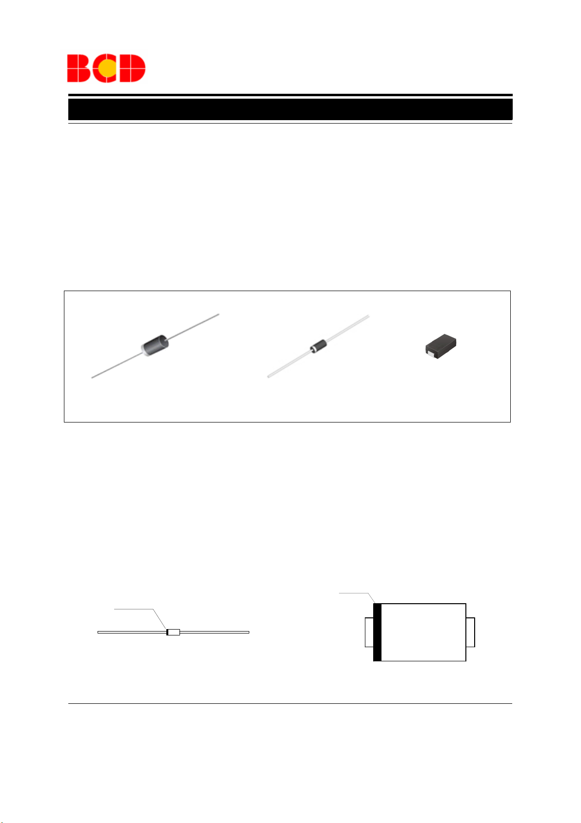
DO-41
Applications
· Low Voltage High Frequency Inverters
· DC-DC Converters
· Free Wheeling
· Polarity Protection
DO-15 DO-214AC
Figure 1. Package Types of APD260
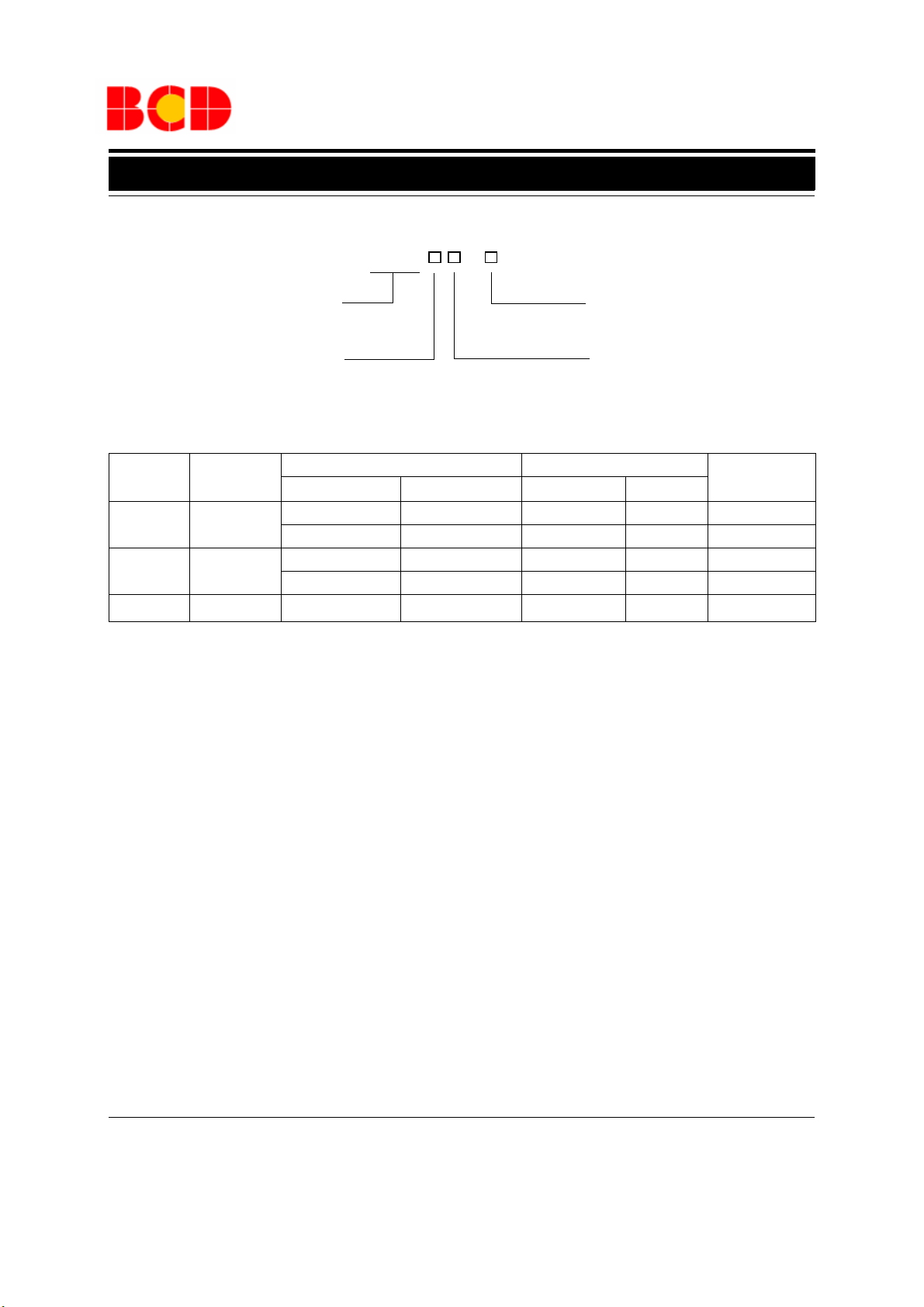
Pin Configuration
VD/VG Package
(DO-41/DO-15)
Cathode line by
Cathode line by
marking
marking
Cathode Anode
Figure 2. Pin Configuration of APD260
Aug. 2011 Rev. 1. 7 BCD Semiconductor Manufacturing Limited
1
VR Package
(DO-214AC)
AnodeCathode
Page 2
Data Sheet
SCHOTTKY BARRIER RECTIFIERS APD260
Ordering Information
APD260 -
Circuit Type
E1: Lead Free
G1: Green
Ammo or Tape & Reel
Package
VD: DO-41
TR:
Blank: Bulk
VG: DO-15
VR: DO-214AC
Package
DO-41
DO-15
DO-214AC
BCD Semiconductor's Pb-free products, as designated with "E1" suffix in the part number, are RoHS compliant. Products with
"G1" suffix are available in green packages.
Temperature
Range
-65 to 125
-65 to 125
-65 to 125
o
C
o
C
o
C
Lead Free
APD260VD-E1 APD260VD-G1 D260VD 260VDG Bulk
APD260VDTR-E1 APD260VDTR-G1 D260VD 260VDG Ammo
APD260VG-E1 APD260VG-G1 D260VG 260VGG Bulk
APD260VGTR-E1 APD260VGTR-G1 D260VG 260VGG Ammo
Part Number Marking ID
Green
APD260VRTR-G1 260VRG Tape & Reel
Lead Free
Green
Packing Type
Aug. 2011 Rev. 1. 7 BCD Semiconductor Manufacturing Limited
2
Page 3

Data Sheet
SCHOTTKY BARRIER RECTIFIERS APD260
Absolute Maximum Ratings (T
=25oC, unless otherwise noted) (Note 1)
A
Parameter Symbol Value Unit
Maximum Repetitive Peak Reverse Voltage V
Maximum DC Blocking Voltage V
Maximum RMS Voltage V
Average Rectified Forward Current
0.375 " (9.5mm) Lead Length (See Figure 3)
I
Non-Repetitive Peak Forward Surge Current
8.3ms Single Half Sine-wave on Rated Load
Operating Junction Temperature Range
Storage Temperature Range
RRM
DC
RMS
F (AV)
I
FSM
T
J
T
STG
60 V
60 V
42 V
2.0 A
50 A
-65 to 125
-65 to 150
o
C
o
C
Note 1: Stresses greater than those listed under "Absolute Maximum Ratings" may cause permanent damage to the device.
These are stress ratings only, and functional operation of the device at these or any other conditions beyond those indicated
under "Recommended Operating Conditions" is not implied. Exposure to "Absolute Maximum Ratings" for extended periods
may affect device reliability.
Aug. 2011 Rev. 1. 7 BCD Semiconductor Manufacturing Limited
3
Page 4

Data Sheet
SCHOTTKY BARRIER RECTIFIERS APD260
Thermal Characteristics (T
=25oC, unless otherwise noted)
A
Parameter Symbol Values Unit
Typical Thermal Resistance
Electrical Characteristics (T
θ
JA
=25oC, unless otherwise noted)
A
DO-41/DO-15 52
DO-214AC 90
Parameter Symbol Values Unit
Forward Voltage @ I
Reverse Current @ Rated V
=2.0A V
F
o
=25
C
T
(Note 2)
R
A
o
=100
T
C
A
F
I
R
0.68 V
0.5
mA
10
Note 2: Pulse Test: 300µs pulse width, 1.0% duty cycle.
o
C/W
Typical Performance Characteristics (T
2.5
2.0
1.5
1.0
0.5
Average Forward Current (A)
Resistive or Inductive Load
0.375''(9.5mm) Lead length
0.0
0 25 50 75 100 125 150
Lead Temperature
o
(
C)
=25oC, unless otherwise noted)
A
10
1
0.1
Instantaneous Forward Current (A)
0.01
0.00.20.40.60.81.01.21.41.6
Instantaneous Forward Voltage (V)
Figure 3. Forward Current Derating Curve Figure 4. Typical Instantaneous Forward Characteristics
T
=25oC
J
TJ=125
o
C
Aug. 2011 Rev. 1. 7 BCD Semiconductor Manufacturing Limited
4
Page 5

Data Sheet
SCHOTTKY BARRIER RECTIFIERS APD260
Typical Performance Characteristics (Continued)
Peak Forward Surge Current (A)
50
45
40
35
30
25
20
15
10
100
TJ=TJ(max)
Single Half Sine-Wave
10 100
Number of Cycles at 60Hz
Figure 5.
Maximum Non-Repetitive Figure 6. Typical Reverse Characteristics
Peak Forward Surge Current
TJ=25oC
f=1.0MHz
=50mVp-p
V
SIG
5
10
4
10
3
10
2
10
1
10
Instantanous Reverse Current (µA)
0
10
0 20406080100
TJ=25oC
TJ=125oC
Percent of Rated Peak Reverse Voltage (%)
Junction Capacitance (pF)
10
0.1 1 10 100
Reverse Voltage (V)
Figure 7. Typical Junction Capacitance
Aug. 2011 Rev. 1. 7 BCD Semiconductor Manufacturing Limited
5
Page 6

Data Sheet
SCHOTTKY BARRIER RECTIFIERS APD260
Mechanical Dimensions
Unit: mm(inch)DO-41
25.400(1. 000) MIN
Cathode line
by marking
25.400(1. 000) MIN
0.700(0.028)
0.900(0.035)
DIA.
4.200(0.165)
5.200(0.205)
2.000(0.080)
2.700(0.107)
DIA.
Aug. 2011 Rev. 1. 7 BCD Semiconductor Manufacturing Limited
6
Page 7

Data Sheet
SCHOTTKY BARRIER RECTIFIERS APD260
Mechanical Dimensions (Continued)
Unit: mm(inch)DO-15
25.400(1.000) MIN
Cathode line
by marking
25.400(1.000) MIN
0.700(0.028)
0.035
0.900( )
DIA.
5.800(0.228)
7.600(0.299)
2.600(0.102)
3.600(0.142)
DIA.
Aug. 2011 Rev. 1. 7 BCD Semiconductor Manufacturing Limited
7
Page 8

Data Sheet
SCHOTTKY BARRIER RECTIFIERS APD260
Mechanical Dimensions (Continued)
Cathode line by
marking
1.250(0.049)
1.650(0.065)
DO-214AC
3. 990(0.157)
4. 600(0.181)
Unit: mm(inch)
2.400(0.094)
2.790(0.110)
0.152(0.006)
0.305(0.012)
1.900(0.075)
2.290(0. 090)
0. 760(0. 030)
1. 520(0. 060)
4.800(0.189)
5.280(0.208)
0.100(0.004)
0.310(0.012)
Aug. 2011 Rev. 1. 7 BCD Semiconductor Manufacturing Limited
8
Page 9

BCD Semiconductor Manufacturing Limited
IMPORTANT NOTICE
IMPORTANT NOTICE
BCD Semiconductor Manufacturing Limited reserves the right to make changes without further notice to any products or specifi-
BCD Semiconductor Manufacturing Limited reserves the right to make changes without further notice to any products or specifi-
cations herein. BCD Semiconductor Manufacturing Limited does not assume any responsibility for use of any its products for any
cations herein. BCD Semiconductor Manufacturing Limited does not assume any responsibility for use of any its products for any
particular purpose, nor does BCD Semiconductor Manufacturing Limited assume any liability arising out of the application or use
particular purpose, nor does BCD Semiconductor Manufacturing Limited assume any liability arising out of the application or use
of any its products or circuits. BCD Semiconductor Manufacturing Limited does not convey any license under its patent rights or
of any its products or circuits. BCD Semiconductor Manufacturing Limited does not convey any license under its patent rights or
other rights nor the rights of others.
other rights nor the rights of others.
http://www.bcdsemi.com
MAIN SITE
MAIN SITE
- Headquarters
BCD Semiconductor Manufacturing Limited
BCD Semiconductor Manufactur ing Limited
- Wafer Fab
No. 1600, Zi Xing Road, Shanghai ZiZhu Science-based Industrial Park, 200241, China
Shanghai SIM-BCD Semiconductor Manufacturing Limited
Tel: +86-21-24162266, Fax: +86-21-24162277
800, Yi Shan Road, Shanghai 200233, China
Tel: +86-21-6485 1491, Fax: +86-21-5450 0008
REGIONAL SALES OFFICE
Shenzhen Office
REGIONAL SALES OFFICE
Shanghai SIM-BCD Semiconductor Manufacturing Co., Ltd., Shenzhen Office
Shenzhen Office
Unit A Room 1203, Skyworth Bldg., Gaoxin Ave.1.S., Nanshan District, Shenzhen,
Shanghai SIM-BCD Semiconductor Manufacturing Co., Ltd. Shenzhen Office
China
Advanced Analog Circuits (Shanghai) Corporation Shenzhen Office
Tel: +86-755-8826 7951
Room E, 5F, Noble Center, No.1006, 3rd Fuzhong Road, Futian District, Shenzhen 518026, China
Fax: +86-755-8826 7865
Tel: +86-755-8826 7951
Fax: +86-755-8826 7865
- Wafer Fab
BCD Semiconductor Manufacturing Limited
Shanghai SIM-BCD Semiconductor Manufacturing Co., Ltd.
- IC Design Group
800 Yi Shan Road, Shanghai 200233, China
Advanced Analog Circuits (Shanghai) Corporation
Tel: +86-21-6485 1491, Fax: +86-21-5450 0008
8F, Zone B, 900, Yi Shan Road, Shanghai 200233, China
Tel: +86-21-6495 9539, Fax: +86-21-6485 9673
Taiwan Office
BCD Semiconductor (Taiwan) Company Limited
Taiwan Office
4F, 298-1, Rui Guang Road, Nei-Hu District, Taipei,
BCD Semiconductor (Taiwan) Company Limited
Tai wan
4F, 298-1, Rui Guang Road, Nei-Hu District, Taipei,
Tel: +886-2-2656 2808
Taiwan
Fax: +886-2-2656 2806
Tel: +886-2-2656 2808
Fax: +886-2-2656 2806
USA Office
BCD Semiconductor Corp.
USA Office
30920 Huntwood Ave. Hayward,
BCD Semiconductor Corporation
CA 94544, USA
30920 Huntwood Ave. Hayward,
Tel : +1-510-324-2988
CA 94544, U.S.A
Fax: +1-510-324-2788
Tel : +1-510-324-2988
Fax: +1-510-324-2788
 Loading...