Diodes APD160 User Manual

Data Sheet
SCHOTTKY BARRIER RECTIFIER APD160
Features
Applications
• Low Forward Voltage Drop
• Very Small Conduction Losses
• High Surge Capability
• Surge Overload Rating to 35A Peak
• Low Voltage High Frequency Inverters
DC-DC Converters
•
• Free Wheeling
• Polarity Protection
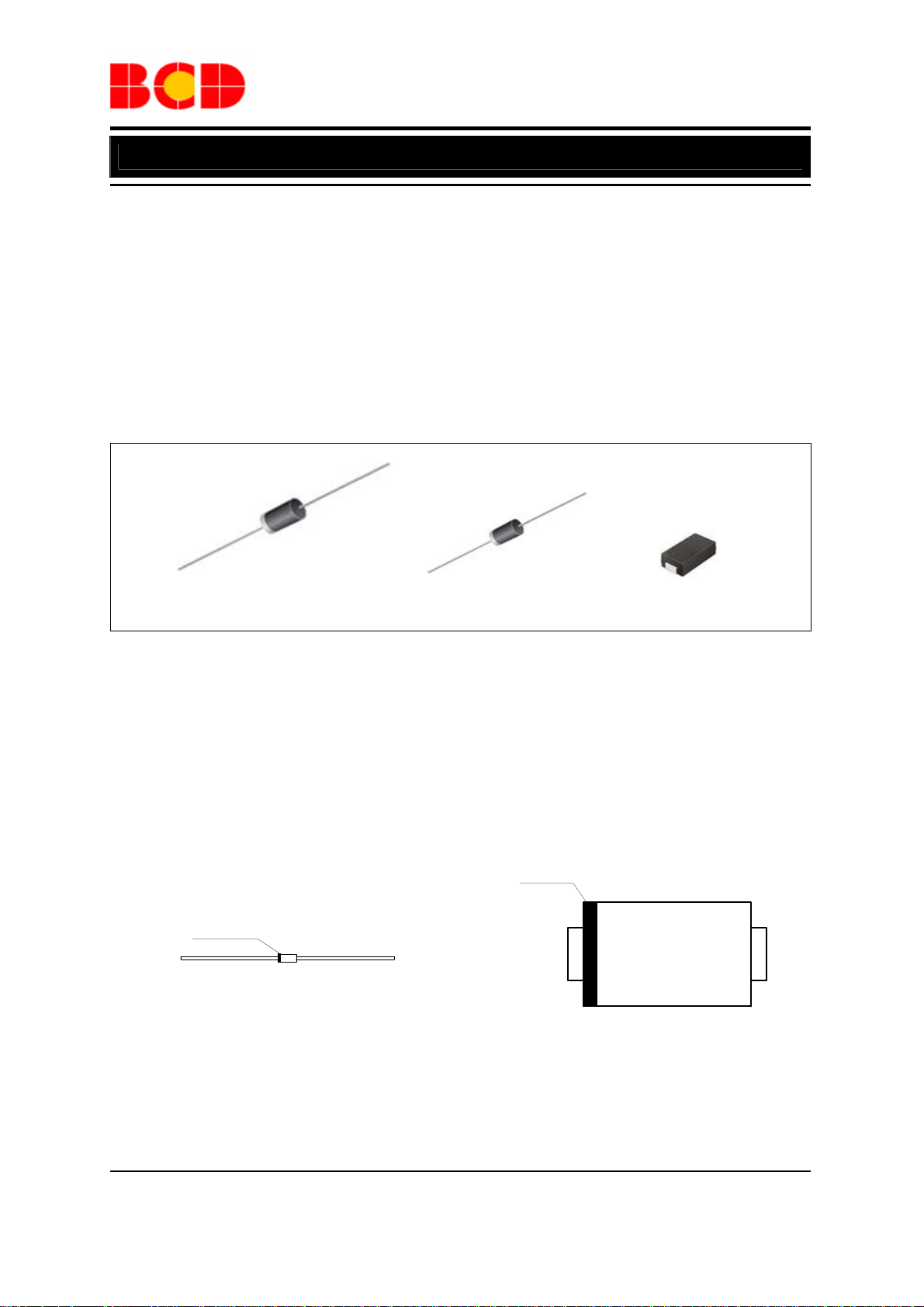
DO-41 R-1 DO-214AC
Figure 1. Package Types of APD160
Pin Configuration
VD/VH Package VR Package
(DO-41/R-1) (DO-214AC)
Cathode line by
marking
Cathode Anode
Figure 2. Pin Configuration of APD160 (Top View)
Cathode line by
marking
Cathode Anode
Aug. 2011 Rev. 1. 7 BCD Semiconductor Manufacturing Limited
1

Data Sheet
SCHOTTKY BARRIER RECTIFIER APD160
Ordering Information
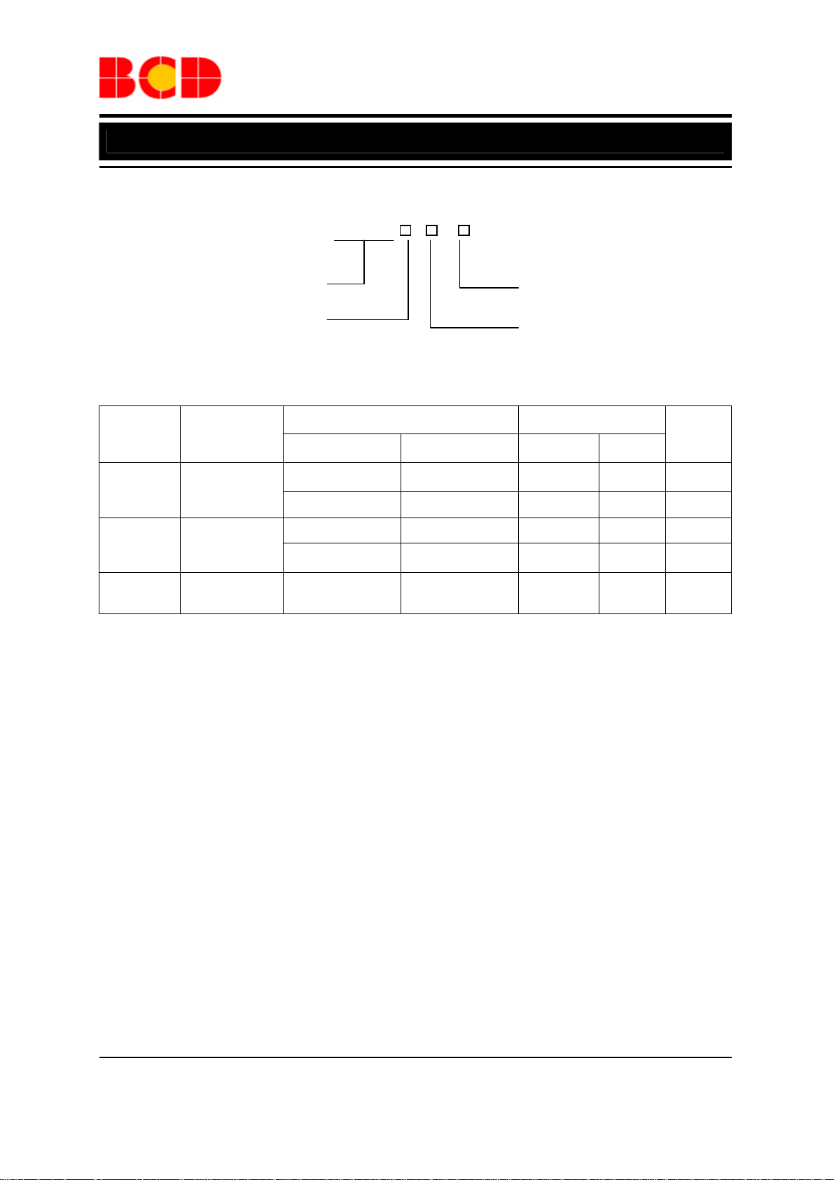
APD160 -
E1: Lead Free
Part Number Marking ID
Packing
Type
Package
Circuit T ype
Package
VD: DO-41
VH: R-1
VR: DO-214AC
Temperature
Range
G1: Green
Blank: Bulk
TR: Ammo or Tape & Reel
Lead Free Green Lead Free Green
DO-41
R-1
DO-214AC
-65 to 125°C
-65 to 125°C
-65 to 125°C
APD160VD-E1 APD160VD-G1 D160VD 160VDG Bulk
APD160VDTR-E1 APD160VDTR-G1 D160VD 160VDG Ammo
APD160VH-E1 APD160VH-G1 D160VH 160VHG Bulk
APD160VHTR-E1 APD160VHTR-G1 D160VH 160VHG Ammo
APD160VRTR-G1 160VRG
Tape &
Reel
BCD Semiconductor's Pb-free products, as designated with "E1" suffix in the part number, are RoHS compliant.
Products with “G1” suffix are available in green packages.
Aug. 2011 Rev. 1. 7 BCD Semiconductor Manufacturing Limited
2

Data Sheet
SCHOTTKY BARRIER RECTIFIER APD160
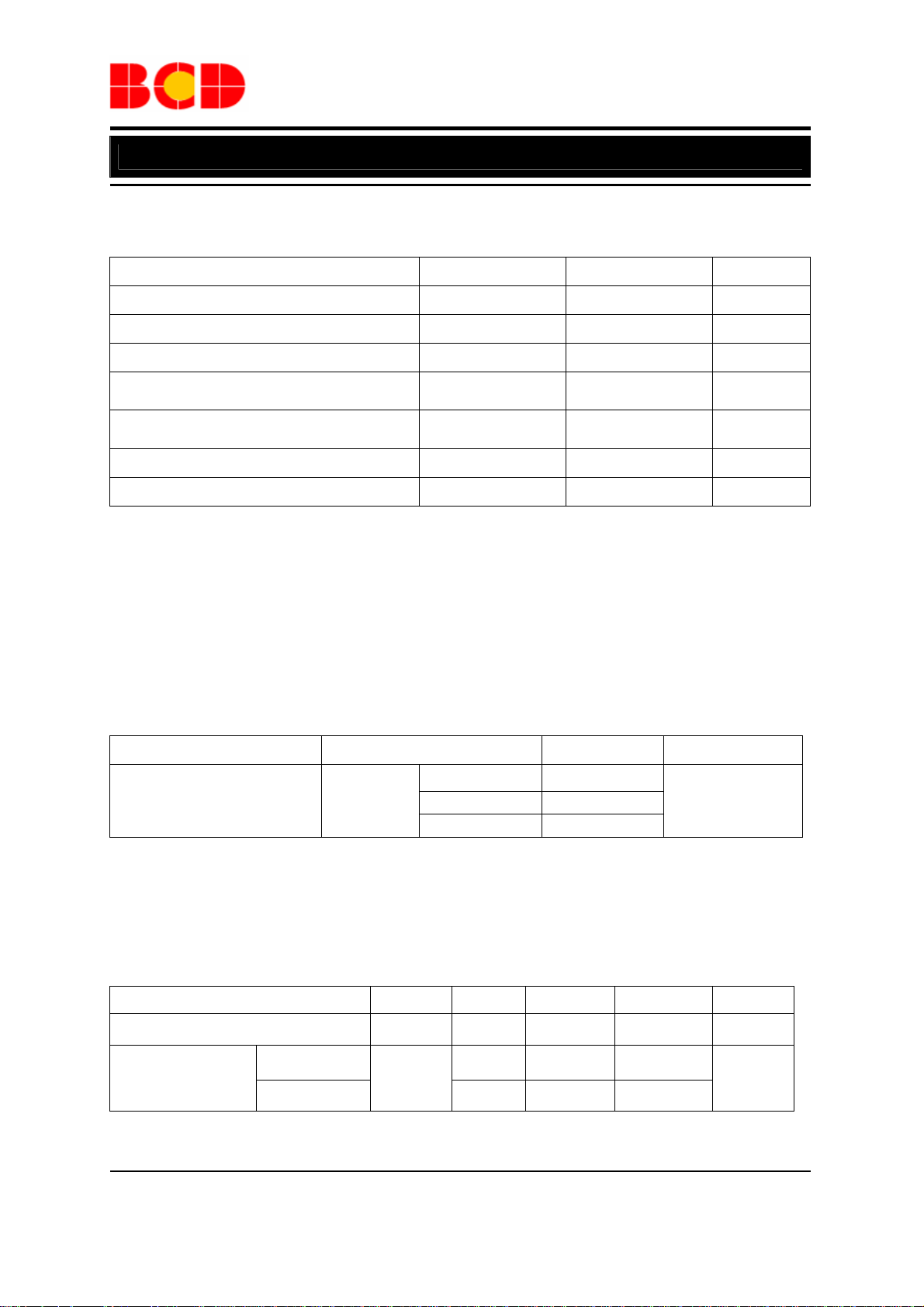
Absolute Maximum Ratings (T
=25°C unless otherwise noted) (Note 1)
A
Parameter Symbol Value Unit
Maximum Repetitive Peak Reverse Voltage V
60 V
RRM
Maximum DC Blocking Voltag e VDC 60 V
Maximum RMS Voltage V
Average Rectified Forward Current
0.375” (9.5mm) Lead Length
Non-repetitive Peak Forward Surge Current
8.3ms Single Half Sine-wave on Rated Load
Operating Junction Temperature Range TJ -65 to 125
Storage Temperature Range T
42 V
RMS
I
1.0 A
F(AV)
35 A
I
FSM
°C
-65 to 150
STG
°C
Note 1: Stresses greater than those listed under “Absolute Maximum Ratings” may cause permanent damage to
the device. These are stress ratings only, and functional operation of the device at these or any other conditions
beyond those indicated under “Recommended Operating Conditions” is not implied. Exposure to “Absolute
Maximum Ratings” for extended periods may affect device reliability.
Thermal Characteristics
(TA=25°C unless otherwise noted)
Parameter Symbol Value Unit
DO-41 80
T ypica l Ther mal Resistance
θ
JA
R-1 80
°C/W
DO-214AC 100
Electrical Characteristics (T
=25°C unless otherwise noted)
A
Parameter Symbol Min Typ Max Unit
Forward Voltage @ IF=1.0A VF 0.68 V
Reverse Current @
Rated V
(Note 2)
R
TA=25°C
=100°C
T
A
I
R
Note 2: Pulse Test: 300µs pulse width, 1.0% duty cycle.
Aug. 2011 Rev. 1. 7 BCD Semiconductor Manufacturing Limited
0.5
mA
10
3
 Loading...