

Page 1
A
OVERVOLTAGE CLAMP
goes
by
Pin Assignments
W-DFN1114-3
1
3
2
Top View
Features
• Wide Input Voltage Range of 3V – 30V
• Ultra-Low Bias Current
• Integrated Low On-Resistance P-Channel FET
• Output Voltage Clamped at 11.15V
• PMOS Protection Mechanism – Removes EMI Issues Typically
Associated with an NMOS Solution
• Supports Reverse Current Operation (USB OTG)
• Available in a W-DFN1114-3 Package
• Totally Lead-Free & Fully RoHS Compliant (Notes 1 & 2)
• Halogen and Antimony Free. “Green” Device (Note 3)
Description
AP9060 is designed to protect the latest generation of PMICs for
portable applications such as Smartphones, UMPCs and others that
utilize battery power.
The device, with its integrated low resistance p-channel MOSFET,
operates as a switch and passes the input voltage through to the
output till the input reaches a clamp voltage limit. Once V
above the clamp limit, which is set to 11.15V, the output voltage gets
clamped and the feedback loop maintains the clamped V
reducing the drive to the p-channel FET.
The output voltage is clamped at 11.15V to ensure that a following
PMIC can detect a faulty charger and ensure safe and proper
communication to the system.
AP9060 also supports reverse operation whereby it can pass up to
1A of current from the PMIC to the load connected to the USB port.
NEW PRODUCT
This makes AP9060 suitable for USB On-The-Go enabled devices.
The AP9060 protection device is available in a low-profile
W-DFN1114-3 package with a typical height of 0.8mm.
IN
OUT
Applications
• Power Interface for New Generation PMICs
• Charger Front-End Protection
• Smartphones
• UMPC
• Portable Applications
Notes: 1. No purposely added lead. Fully EU Directive 2002/95/EC (RoHS) & 2011/65/EU (RoHS 2) compliant.
2. See http://www.diodes.com for more information about Diodes Incorporated’s definitions of Halogen- and Antimony-free, "Green" and Lead-free.
3. Halogen- and Antimony-free "Green” products are defined as those which contain <900ppm bromine, <900ppm chlorine (<1500ppm total Br + Cl) and
<1000ppm antimony compounds.
P9060
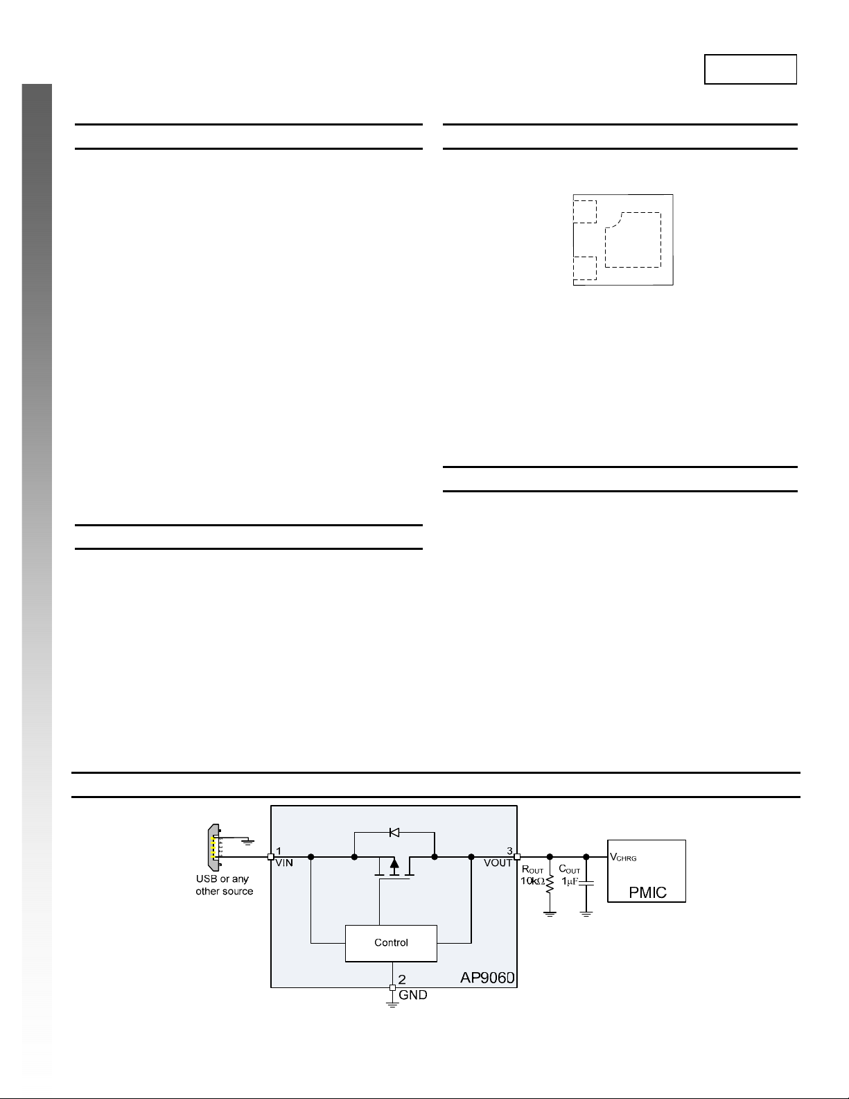
Typical Applications Circuit
AP9060
Document number: DS36001 Rev. 2 - 2
Figure 1 Typical Application Circuit
1 of 9
www.diodes.com
August 2012
© Diodes Incorporated
Page 2

A
Pin Descriptions
Pin
Number
1 VIN Input voltage to the device.
2 GND System ground.
3/PAD VOUT Output loltage, which follows VIN and gets clamped if VIN exceeds the clamp voltage of 11.15V (typ).
Pin
Name
Function
Functional Block Diagram
P9060
NEW PRODUCT
Absolute Maximum Ratings (Note 4) (@T
Notes: 4. Stresses greater than the 'Absolute Maximum Ratings' specified above may cause permanent damage to the device. These are stress ratings only;
functional operation of the device at these or any other conditions exceeding those indicated in this specification is not implied. Device reliability may be
affected by exposure to absolute maximum rating conditions for extended periods of time.
5. Semiconductor devices are ESD sensitive and may be damaged by exposure to ESD events. Suitable ESD precautions should be taken when handling
and transporting these devices.
AP9060
Document number: DS36001 Rev. 2 - 2
Symbol Parameter Rating Unit
VIN Input Supply Voltage -0.3 to +30 V
Maximum Continuous Switch Current (Note 6)
I
MAX
PD Power Dissipation @ TA = +25°C (Note 6) 1.1 W
TJ Junction Temperature Range -40 to +125 °C
T
Storage Temperature Range -55 to +150 °C
STG
TL Maximum Lead Temperature for Soldering Purposes 260 °C
ESD Susceptibility (Note 5)
HBM Human Body Model 8.0 kV
MM Machine Model 350 V
TA = +25°C
T
= +85°C
A
Figure 2 Functional Block Diagram
= +25°C, unless otherwise specified.)
A
2 of 9
www.diodes.com
2.6
1.6
A
August 2012
© Diodes Incorporated
Page 3

A
Thermal Resistance (Note 6)
Symbol Parameter Rating Unit
θ
Junction to Ambient 85 °C/W
JA
Note: 6. Surface mounted on JEDEC’s High Effective Thermal Conductivity Test Board (JESD51-7).
Recommended Operating Conditions (Note 7) (@T
= +25°C, unless otherwise specified.)
A
Symbol Parameter Min Max Unit
VIN Supply Voltage 3 30 V
TA Operating Ambient Temperature Range −40 +85 °C
Note: 7. The device function is not guaranteed outside of the recommended operating conditions.
Electrical Characteristics (@T
NEW PRODUCT
AP9060 is tested at V
= 5V, I
IN
= 0mA, unless otherwise noted.
OUT
= +25°C, unless otherwise specified.)
A
Symbol Parameter Test Conditions Min Typ Max Unit
V
Output clamp voltage VIN = 30V 10.8 11.15 11.5 V
CLAMP
= 5V, I
V
RON On-Resistance (Note 8)
Vpk Peak Output Voltage (Note 9)
I
Input Bias Current
bias
THMSD Thermal Shutdown Threshold (Note 9) R
THM
V
OUT_REV
I
IN_REV
T
start
Notes: 8. Pulse tested with a width of 20ms.
9. Guaranteed by design.
10. To support reverse power operation, as in the case of USB OTG systems. A voltage source is connected to V
Thermal Shutdown Hysteresis(Note 9) R
hyst
Reverse Supply Voltage on VOUT(Note 10) IIN = −500mA 3.0 5.0 8.0 V
Reverse Load Current on VIN (Note 10)
Soft-Start Time VIN = 5V 10 ms
IN
= 3V, I
V
IN
goes from 0V to 30V with 100ns
V
IN
rise time, C
= 5V
V
IN
V
= 30V
IN
= 10kΩ 140 °C
OUT
= 10kΩ 20 °C
OUT
V
= 5V −500 −1000 mA
OUT
= 1000mA
OUT
= 1000mA
OUT
= 100nF
OUT
AP9060
Document number: DS36001 Rev. 2 - 2
3 of 9
www.diodes.com
P9060
90
105
16.0 V
OUT
5
25
and a load connected on VIN.
120
139
6
31
© Diodes Incorporated
mΩ
µA
August 2012
Page 4

A
Typical Performance Characteristics
12
TA= 25°C
NEW PRODUCT
(V)
V
OUT
11
10
9
8
7
6
5
4
3
2
1
0
= 10kΩ
R
OUT
0 2 4 6 81012141618202224262830
VIN(V)
Figure 3 V
OUT
vs. VIN
12.0
11.8
11.6
11.4
11.2
(V)
11.0
CLAMP
10.8
V
10.6
10.4
10.2
10.0
-40-200 20406080100120
TEMPERATURE (°C)
Figure 4 Output Clamp Voltage vs. Temperature
P9060
VIN= 30V
I
= 0A
OUT
140
130
120
110
100
90
ON RESISTANCE (mΩ)
80
70
60
VIN(V)
I
= 1A (pulsed)
OUT
85°C
50°C
25°C
0°C
−25°C
−40°C
Figure 5 On-Resistance vs. VIN and Temperature
1.4
VIN= 5V
1.3
I
OUT
= 1A
1.2
1.1
1
0.9
0.8
0.7
ON RESISTANCE (NORMALIZED)
0.6
-40 -20 0 20 40 60 80 100 120
TEMPERATURE (°C)
Figure 7 On-Resistance (normalized) vs. Temperature
AP9060
Document number: DS36001 Rev. 2 - 2
130
120
110
100
90
80
ON RESISTANCE (mΩ)
70
109876543
60
Figure 6 On-Resistance vs. I
16
14
12
10
8
6
4
LEAKAGE CURRENT (µA)
2
0
Figure 8 FET Leakage Current (in thermal shutdown) vs. V
4 of 9
www.diodes.com
VIN= 5V
85°C
50°C
25°C
0°C
−25°C
−40°C
25 175 325 475 625 775 925
I
(mA)
OUT
R
= 10kΩ
OUT
Temperature = 150° C
and Temperature
OUT
Device in thermal shutdown mode
3 6 9 12151821242730
VIN(V)
© Diodes Incorporated
IN
August 2012
Page 5

A
Application Information
Over-Voltage Protection
AP9060 protects sensitive circuits by clamping the input voltage to a safe level. In other words, AP9060 conditions the input voltage before
presenting it to the sensitive circuitry.
The clamp voltage on AP9060 is set to 11.15V (typically at room temperature). Therefore, the sensitive circuitry will not be exposed to a voltage
greater than 11.15V. As a consequence, it is important to ensure that the sensitive ICs that follow AP9060 are safe to operate u p to the clamp
voltage level (refer to Figure 4 for variation in clamp voltage over temperature).
If the input voltage is below V
is the current drawn by the sensitive ICs). On the other hand, if V
ensure that the voltage on VOUT is maintained at the clamp level.
, the PMOS pass transistor in the AP9060 fully turns on and only I x R
CLAMP
is greater than the clamp voltage, then AP9060 limits the drive to the FET to
IN
Over-Temperature Protection
As a secondary protection mechanism, AP9060 incorporates an over-temperature shutdown feature. Therefore, if the sensitive circuitry draws
too much current either in normal mode or in the clamp mode, AP9060 will turn off the PMOS transistor, provided the junction temperature
exceeds the thermal shutdown threshold (THM
– THM
THM
SD
In the clamp mode, given that any input voltage above V
NEW PRODUCT
power dissipation within AP9060 in check by minimising the current drawn in this mode.
hyst
.
). Thereafter, the device will resume normal operation once the junction temperature falls below
SD
is dropped across the pass transistor in AP9060, care must be taken to keep the
CLAMP
Fast Input Transient Protection
AP9060 will also protect the sensitive circuits against fast input transients. Upon detecting a fast transient on VIN, AP9060 reduces the drive to
the FET in order to minimise the overshoot on VOUT. With 100nF on VOUT, if the voltage on VIN goes from 0V to 30V in 100ns, the output
voltage will not peak above V
.
pk
Reverse Operation
AP9060 supports the USB OTG specification and can operate in the reverse direction as well. Therefore, if the sensitive circuitry drives a voltage
on VOUT (V
dropped across the device, similar to the forward operation.
However, note that neither over-voltage nor over-temperature protection mechanisms will function in this mode.
) and a load is connected on VIN (I
OUT_REV
), then AP9060 will turn the FET on in the reverse direction and only I x RON will be
IN_REV
Output Capacitor
It is recommended to have a capacitor on VOUT in a range between 100nF and 10µF.
Output Resistor
It is recommended to have a resistor on VOUT in a range between 10kΩ and 100kΩ.
is dropped across the FET (where, I
ON
P9060
AP9060
Document number: DS36001 Rev. 2 - 2
5 of 9
www.diodes.com
August 2012
© Diodes Incorporated
Page 6

A
Ordering Information
P9060
AP9060 XYZ-7
Package
FM8 : W-DFN1114-3
Part Number
AP9060FM8-7 FM8 W-DFN1114-3 3000/Tape & Reel -7
Note: 11. Pad layout as shown on Diodes Inc. suggested pad layout document AP02001, which can be found on our website at
http://www.diodes.com/datasheets/ap02001.pdf.
NEW PRODUCT
Package
Code
Packaging
(Note 11)
Packing
-7 : Tape and Reel
7” Tape and Reel
Quantity Part Number Suffix
Marking Information
W-DFN1114-3
( Top View )
XXX : Identification code
Y
XX
Y W X
Device Package Identification Code
AP9060FM8-7 W-DFN1114-3 CZ
: Year 0~9
W
: Week : A~Z : 1~26 week;
a~z : 27~52 week; z represents
52 and 53 week
X
: A~Z : Internal Code
AP9060
Document number: DS36001 Rev. 2 - 2
6 of 9
www.diodes.com
August 2012
© Diodes Incorporated
Page 7

A
Package Outline Dimensions (All dimensions in mm.)
W-DFN1114-3
A
b︵2
1
A
x
︶
3
Seating Plane
L
NEW PRODUCT
A
Pin #1 ID
E
0.265
︵
E
1
D
e
︶
R
0
.
1
5
0
D
1
Suggested Pad Layout
W-DFN1114-3
Y
2
X
1
Y
1
X
Y
C
X
2
P9060
W-DFN1114-3
Dim Min Max Typ
A 0.77 0.83 0.80
A1 0 0.05 0.02
A3 - - 0.152
b 0.25 0.35 0.30
D 1.05 1.15 1.10
D1 0.70 0.80 0.75
e - - 0.55
E 1.35 1.45 1.40
E1 0.66 0.76 0.71
L 0.20 0.30 0.25
All Dimensions in mm
Dimensions
C 0.55.
X 0.400
X1 0.750
X2 0.950
Y 0.450
Y1 0.710
Y2 1.375
Value
(in mm)
AP9060
Document number: DS36001 Rev. 2 - 2
7 of 9
www.diodes.com
August 2012
© Diodes Incorporated
Page 8

r
n
p
2
D
t
m
t
w
m
h
m
c
p
2
e
A
2
P9060
NEW PRODUCT
Tape Orie
tation
(All
imensions in
m.) (Note 12)
Pin 1 i
ndicator
Note: 12. The ta
AP9060
Document numbe
ing orientation of
: DS36001 Rev.
he other package
- 2
type can be found
on our website at
8 of 9
ww.diodes.co
ttp://www.diodes.
om/datasheets/a
02007.pdf
August 201
© Diodes Incorporat
d
Page 9

A
DIODES INCORPORATED MAKES NO WARRANTY OF ANY KIND, EXPRESS OR IMPLIED, WITH REGARDS TO THIS DOCUMENT,
INCLUDING, BUT NOT LIMITED TO, THE IMPLIED WARRANTIES OF MERCHANTABILITY AND FITNESS FOR A PARTICULAR PURPOSE
(AND THEIR EQUIVALENTS UNDER THE LAWS OF ANY JURISDICTION).
Diodes Incorporated and its subsidiaries reserve the right to make modifications, enhancements, improvements, corrections or other changes
without further notice to this document and any product described herein. Diodes Incorporated does not assume any liability arising out of the
application or use of this document or any product described herein; neither does Diodes Incorporated convey any license under its patent or
trademark rights, nor the rights of others. Any Customer or user of this document or products described herein in such applications shall assume
all risks of such use and will agree to hold Diodes Incorporated and all the companies whose products are represented on Diodes Incorporated
website, harmless against all damages.
Diodes Incorporated does not warrant or accept any liability whatsoever in respect of any products purchased through unauthorized sales channel.
Should Customers purchase or use Diodes Incorporated products for any unintended or unauthorize d application, Customers shall indemnify and
hold Diodes Incorporated and its representatives harmless against all claims, damages, expenses, and attorney fees arising out of, directly or
indirectly, any claim of personal injury or death associated with such unintended or unauthorized application.
Products described herein may be covered by one or more United States, international or foreign patents pending. Product names and markings
noted herein may also be covered by one or more United States, international or foreign trademarks.
NEW PRODUCT
Diodes Incorporated products are specifically not authorized for use as critical components in life support devices or systems without the express
written approval of the Chief Executive Officer of Diodes Incorporated. As used herein:
A. Life support devices or systems are devices or systems which:
1. are intended to implant into the body, or
labeling can be reasonably expected to result in significant injury to the user.
B. A critical component is any component in a life support device or system whose failure to perform can be reasonably expected to cause the
failure of the life support device or to affect its safety or effectiveness.
Customers represent that they have all necessary expertise in the safety and regulatory ramifications of their life support devices or systems, and
acknowledge and agree that they are solely responsible for all legal, regulatory and safety-related requirements concerning their products and any
use of Diodes Incorporated products in such safety-critical, life support devices or systems, notwithstanding any devices- or systems-related
information or support that may be provided by Diodes Incorporated. Further, Customers must fully indemnify Diodes Incorporated and its
representatives against any damages arising out of the use of Diodes Incorporated products in such safety-critical, life support devices or systems.
Copyright © 2012, Diodes Incorporated
www.diodes.com
2. support or sustain life and whose failure to perform when properly used in accordance with instructions for use provided in the
IMPORTANT NOTICE
LIFE SUPPORT
P9060
AP9060
Document number: DS36001 Rev. 2 - 2
9 of 9
www.diodes.com
August 2012
© Diodes Incorporated
 Loading...