

Page 1
AP9050
PROTECTION INTERFACE for PMICs with
INTEGRATED OVP CONTROL
Description
AP9050 is designed to protect the latest generation of PMICs
for portable applications such as UMPCs, smartphones and
others utilizing battery power.
The integrated LDO allows the PMIC to power up and
determine whether the connected power supply (USB or
AC-DC wall adapter) is valid and a safe operation can be
performed.
The PMIC controls the operation of the integrated n-channel
MOSFET to either pass the line voltage or disconnect the line
from the PMIC to protect its internal circuits in the event of an
over-voltage.
The AP9050 is available in a low-profile U-DFN2020-6
package.
NEW PRODUCT
Features
• Input Supply Range from 3V to 30V
• Lower Power Dissipation and Higher Efficiency as
compared to a Zener Shunt Regulator
• LDO is stable without a bypass capacitor on the output
and operates across the temperature range
• Available in a U-DFN2020-6 package with a typical
height of 0.575mm
Note: 1. EU Directive 2002/95/EC (RoHS). All applicable RoHS exemptions applied. Please visit our website at
http://www.diodes.com/products/lead_free.html.
Pin Assignments
Applications
• Power Interface for New Generation PMICs
• Charger Front End Protection
• Smartphone
• Cell Phone
• Ultra Mobile PC
• Tablets
(Top View)
1
2
3
8
7
U-DFN2020-6
6
5
4
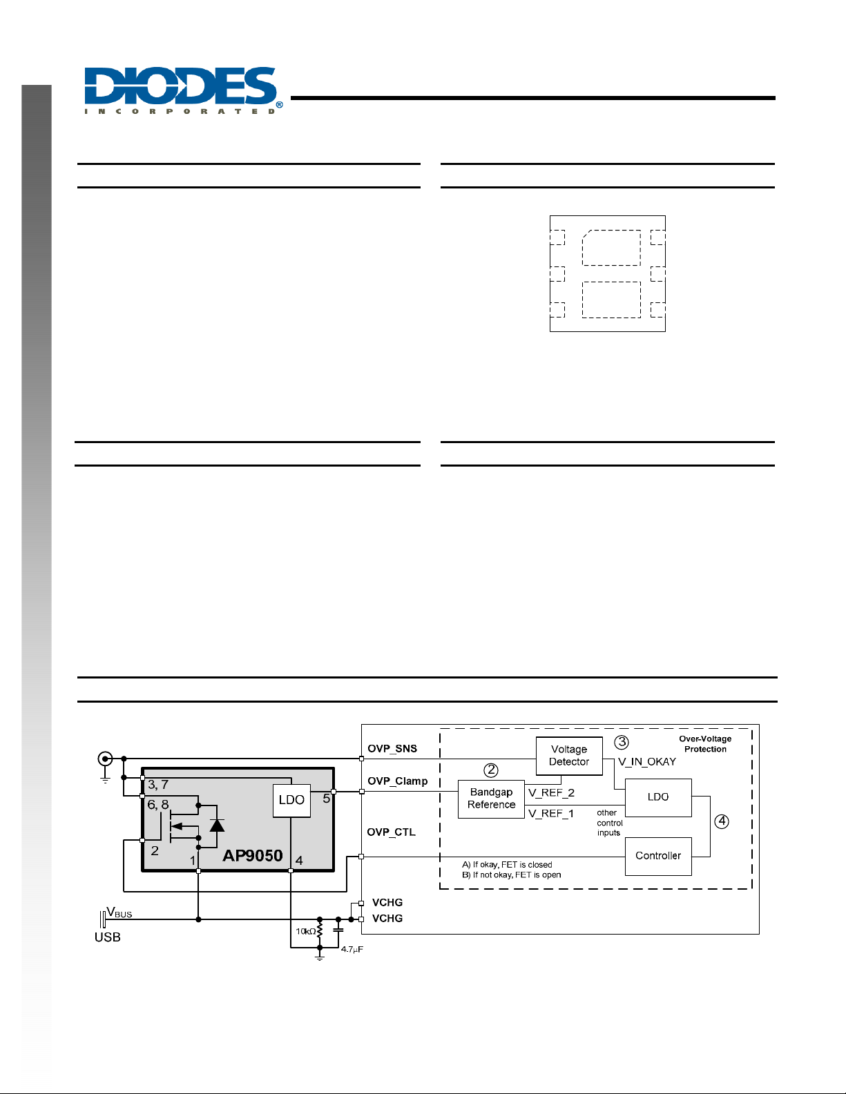
Typical Application Circuit
AP9050
Document number: DS35283 Rev. 1 - 2
Figure 1. Typical Application Circuit
1 of 9
www.diodes.com
March 2011
© Diodes Incorporated
Page 2
PROTECTION INTERFACE for PMICs with
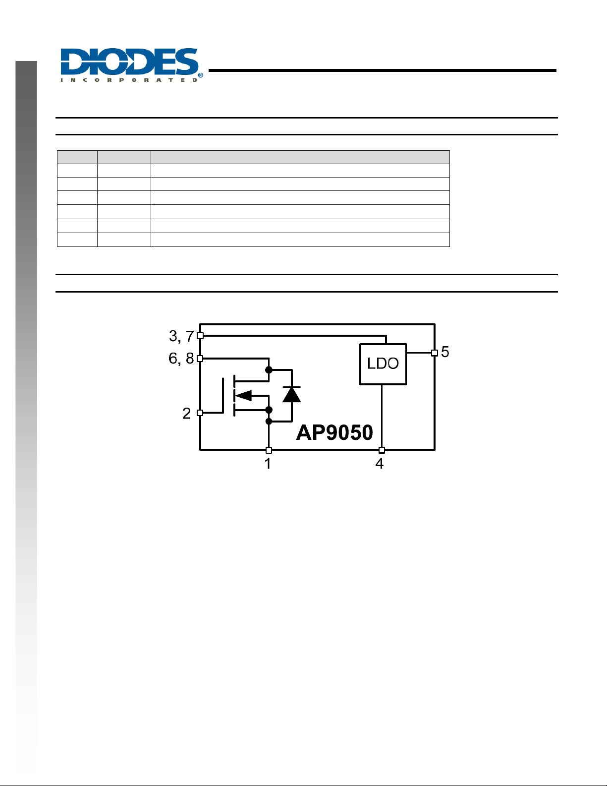
Pin Descriptions
Pin # Name Description
1 Source Source of the n-channel power FET. Pass-switch’s output pin.
2 Gate Gate of the FET switch. Pass-switch’s control pin.
V
V
IN
OUT
Input voltage to the internal LDO.
Output of the LDO.
3, 7
4 Ground LDO ground connection.
5
6, 8 Drain Drain of the power FET. Pass-switch’s input pin.
Functional Block Diagram
AP9050
INTEGRATED OVP CONTROL
NEW PRODUCT
Figure 2. Functional Block Diagram
AP9050
Document number: DS35283 Rev. 1 - 2
2 of 9
www.diodes.com
March 2011
© Diodes Incorporated
Page 3
PROTECTION INTERFACE for PMICs with
INTEGRATED OVP CONTROL
Absolute Maximum Ratings (Note 2, 3)
Symbol Parameter Rating Unit
VIN
VGS
I
Dpk
ID
P
max
TJ
NEW PRODUCT
Semiconductor devices are ESD sensitive and may be damaged by exposure to ESD events. Suitable ESD precautions should be taken when handling and
transporting these devices.
Notes: 2. Exceeding these ratings may damage the device.
3. Mounted on FR4 Board using 30 mm
TJ
TL
4. Dual die operation (equally−heated).
Supply Voltage
Gate-to-Source Voltage ±12 V
Drain Current, Peak (10µs pulse) 19 A
Drain Current, Continuous
(Note 4, Steady-State)
= 25ºC
T
A
T
= 85ºC
A
Total Power Dissipation @ TA = 25°C
(Note 3, 4)
Junction Temperature Range −40 to +125 °C
Non-operating Temperature Range −55 to +150 °C
Maximum Lead Temperature for Soldering
Purposes
2
, 2 oz Cu.
−0.3 to 30
3.7
2.7
750 mW
260 °C
AP9050
V
A
Thermal Resistance
Symbol Parameter Rating Unit
θ
JA
θ
JC
Note: 5. Test condition for DFN2020-6: Mounted on FR4 Board using 30 mm2, 2 oz Cu.
Junction to Ambient (Note 5) 132 °C/W
Junction to Case 13 °C/W
Recommended Operating Conditions (Note 6)
Symbol Parameter Min Max Unit
VIN
TA
Note: 6. The device function is not guaranteed outside of the recommended operating conditions.
Supply Voltage
Operating Ambient Temperature Range
3
−40
30 V
+85 °C
AP9050
Document number: DS35283 Rev. 1 - 2
3 of 9
www.diodes.com
March 2011
© Diodes Incorporated
Page 4

AP9050
PROTECTION INTERFACE for PMICs with
INTEGRATED OVP CONTROL
Electrical Characteristics (V
Symbol Parameter Test Conditions Min Typ. Max Unit
Power FET
I
Zero Gate Voltage Drain Current
Gate-to-Source Leakage Current
Gate Threshold Voltage
Drain-to-Source On-Resistance
(Note 7)
Forward Transconductance
Input Capacitance
I
V
GS(th)
R
DS(on)
gFS
C
DSS
GSS
ISS
NEW PRODUCT
C
OSS
C
RSS
LDO (unless otherwise noted, TJ = 25ºC, VIN = 5.0V)
V
OUT
V
head
Response to Input Transient
t
pulse
Vpk
Total Device
I
bias
V
IN_min
Notes: 7. Pulse test width 300µs, duty cycle 2%
8. Guaranteed by design
Output Capacitance
Reverse Transfer Capacitance
Regulated Output Voltage
Headroom
Time signal is above 5.5V
Peak Voltage
Input Bias Current
Minimum Operating Voltage 3.0 V
(OVP_SENSE) = 5.0V, TJ = +25°C, unless otherwise noted)
IN
= 24V, VGS = 0V
V
DS
T
= 85°C
J
VDS = 0V, VGS = ±8V
VGS = VDS, ID = 250µA
= 4.5V, ID = 2.0A
V
GS
V
= 2.5V, ID = 2.0A
GS
VDS = 5V, ID = 2.0A
VDS = 15V, VGS = 0V,
f = 1MHz
VDS = 15V, VGS = 0V,
f = 1MHz
= 15V, VGS = 0V,
V
DS
f = 1MHz
VIN = 5.5V, I
VIN − V
OUT
V
= 4.6V
IN
VIN − V
OUT
= 4.8V, TJ = −40 to +125°C
V
IN
, I
, I
OUT
OUT
OUT
= 1mA
= 1.2mA,
= 10mA,
VIN 0 to 30V, < 1µs rise time,
5.0kΩ resistive load (Note 8)
VIN 0 to 30V, < 1µs rise time,
5.0kΩ resistive load (Note 8)
VIN = 5.5V
80 nA
0.62 0.9 1.2 V
41
55
8 S
500 pF
65 pF
50 pF
4.6 5.0 5.3 V
150 mV
1000 mV
5.0 µs
9.0 V
110 850 µA
1.0
10
53
68
µA
mΩ
AP9050
Document number: DS35283 Rev. 1 - 2
4 of 9
www.diodes.com
March 2011
© Diodes Incorporated
Page 5

Typical Performance Characteristics
1.6
1.5
1.4
1.3
DS(on)
1.2
1.1
1
0.9
Normali sed R
0.8
0.7
0.6
-50 -25 0 25 50 75 100 125 150
NEW PRODUCT
Figure 3. R
20
VGS=10V
18
16
14
12
10
8
6
Drain Cur rent (A)
4
2
0
012345
5.2
VGS=4.5V
=2A
I
D
Junction T e mper atur e (ºC)
variation over junction temperature
DS(ON)
VGS=3V
Drain-Source Voltage (V)
Figure 4. R
DS(ON)
AP9050
PROTECTION INTERFACE for PMICs with
INTEGRATED OVP CONTROL
VGS=2.5V
VGS=2V
VGS=1.5V
Characteristics
Figure 5. Output voltage variation over junction temperature
AP9050
Document number: DS35283 Rev. 1 - 2
5.15
5.1
5.05
5
4.95
Output Voltage (V)
4.9
4.85
4.8
-50 -25 0 25 50 75 100 125 150
Junction Temperature (ºC)
5 of 9
www.diodes.com
March 2011
© Diodes Incorporated
Page 6

Applications Information
Theory of Operation
The AP9050 was designed to work in close relationship
with a PMIC (Power Management IC). To protect the
PMIC from an overvoltage situation the AP9050 powers up
a detection circuit within the connected PMIC. (See Figure
2 as reference)
This detection circuit determines if a valid input source is
connected (ex. V
the power MOSFET will be turned on and the supply
current to the PMIC will be turned on. The overvoltage
detection is continuous, if an overvoltage occurs at a later
state the Power MOSFET will be turned off.
NEW PRODUCT
PCB Layout
The AP9050 was designed utilizing two process
technologies to provide best performance and a cost
effective solution.
< 8V). If a valid input source is detected
IN
AP9050
PROTECTION INTERFACE for PMICs with
INTEGRATED OVP CONTROL
External Capacitors
AP9050 was specified to reduce board space and external
component count, by designing the LDO to be stable
without an external bypass capacitor.
A low ESR 1nF to 10nF external capacitor can be used to
improve behavior with fast ac transients or other switching
currents that might be present.
To improve noise immunity and ac impedance from lon g
input traces a 1nF capacitor can be added to the input V
of the LDO.
IN
1
2
3
6
8
5
7
4
Figure 6. Package Pin Out
Both die are packaged side by side in the U-DFN2020-6
package and are mounted on two separate exposed pads.
These pads are not required for electrical functionality, but
to aid with the thermal performance of AP9050.
Attention should be paid in the layout of the PCB (Printed
Circuit Board) that PAD7 is connected to V
pin 3, while PAD8 is connected to the Drain of the Power
MOSFET, pin 6 of the package. For best thermal
performance large copper areas connected to the two
exposed pads should be used to transfer heat away from
the AP9050.
of the LDO,
IN
AP9050
Document number: DS35283 Rev. 1 - 2
6 of 9
www.diodes.com
March 2011
© Diodes Incorporated
Page 7

Ordering Information
AP9050
PROTECTION INTERFACE for PMICs with
INTEGRATED OVP CONTROL
AP9050FDB-7
Package
U-DFN2020-6
Packing
FDB
Device
AP9050FDB-7 FDB U-DFN2020-6 3000/Tape & Reel -7
Note: 10. Pad layout as shown on Diodes Inc. suggested pad layout document AP02001, which can be found on our website at
http://www.diodes.com/datasheets/ap02001.pdf.
NEW PRODUCT
Package
Code
Packaging
(Note 10)
Quantity Part Number Suffix
7” Tape and Reel
Marking Information
U-DFN2020-6
( Top View )
XX : Identification Code
: Year : 0~9
X X
W
XY
Y
W
: Week : A~Z : 1~26 week;
a~z : 27~52 week; z represents
52 and 53 week
X
: A~Z : Internal code
Device Package Identification Code
AP9050FDB U-DFN2020-6 BZ
AP9050
Document number: DS35283 Rev. 1 - 2
7 of 9
www.diodes.com
March 2011
© Diodes Incorporated
Page 8

PROTECTION INTERFACE for PMICs with
Package Outline Dimensions (All Dimensions in mm)
U-DFN2020-6
AP9050
INTEGRATED OVP CONTROL
NEW PRODUCT
Marking
1.95/2.075
0.13Typ.
A
0.25/0.35
0.2/0.3
0.43mon.
(Active area depth)
Seating plane
C
6x-0.45
6x-0.3
Land Pattern Recommendation
0.05
M C A B
C
L
1.05
2x-0.70
C
L
0.65
Top View
unit:mm
1.7
2x-1.10
2x-
0.05 C
0.08 C
0.15 C
0.545/0.605
B
1.95/2.075
0.65nom.
C
0.15
0/0.05
2x
2x-0.5/0.7 0.45
R0.15
Pin#1 ID
2x-0.9/1.1
1
.
0
R
Bottom View
AP9050
Document number: DS35283 Rev. 1 - 2
8 of 9
www.diodes.com
March 2011
© Diodes Incorporated
Page 9

NEW PRODUCT
AP9050
PROTECTION INTERFACE for PMICs with
INTEGRATED OVP CONTROL
IMPORTANT NOTICE
DIODES INCORPORATED MAKES NO WARRANTY OF ANY KIND, EXPRESS OR IMPLIED, WITH REGARDS TO THIS
DOCUMENT, INCLUDING, BUT NOT LIMITED TO, THE IMPLIED WARRANTIES OF MERCHANTABILITY A ND FITNESS FOR A
PARTICULAR PURPOSE (AND THEIR EQUIVALENTS UNDER THE LAWS OF ANY JURISDICTION).
Diodes Incorporated and its subsidiaries reserve the right to make modifications, enhancements, improvements, corrections or other
changes without further notice to this document and any product described herein. Diodes Incorporat ed does not assume any liability
arising out of the application or use of this document or any product described herein; neither does Diodes Incorporated convey any
license under its patent or trademark rights, nor the rights of others. A ny Customer or user of this document or products described
herein in such applications shall assume all risks of such use and will agree to hold Diodes Incorporated and all the companies
whose products are represented on Diodes Incorporated website, harml ess ag ai nst all damages.
Diodes Incorporated does not warrant or acc ept any liability whatsoever in respec t of any products purchas ed through unauthorized
sales channel.
Should Customers purchase or use Diodes Incorporated products for any unintended or unauthorized application, Customers shall
indemnify and hold Diodes Incorporated and its representatives harmless agai nst all claims, damages, expenses, and attorney fees
arising out of, directly or indirectly, any claim of personal injury or death ass ociated with such unintended or unauthorized application.
Products described herein may be covered by one or more United Stat es, international or foreign patents pending. Product names
and markings noted herein may also be covered by one or more United States, international or foreign trademarks.
LIFE SUPPORT
Diodes Incorporated products are specifically not authorized for use as critical components in life support devices or systems without
the express written approval of the Chief Executive Officer of Diodes Incorporated. As used herei n:
A. Life support devices or systems are devices or systems which:
1. are intended to implant into the body, or
2. support or sustain life and whose failure to perform when properly used in accordance with instructi ons for us e provided
in the labeling can be reasonably expected to result in significant injury to the user.
B. A critical component is any component in a life support device or system whose failure t o perform can be reasonably expected
to cause the failure of the life support device or to affect its safety or effectiveness .
Customers represent that they have all necessary expertise in the safety and regulatory ramifications of their life support devices or
systems, and acknowledge and agree that they are solely responsible for all legal, regulatory and safety-related requirements
concerning their products and any use of Diodes Incorporated products in such safety-critical, life support devices or systems,
notwithstanding any devices- or systems-related information or support that may be provided by Diodes Incorporated. Further,
Customers must fully indemnify Diodes Incorporated and its representatives agai nst any damages arising out of the use of Diodes
Incorporated products in such safety-critic al, l ife support devic es or syst ems .
Copyright © 2011, Diodes Incorporated
www.diodes.com
AP9050
Document number: DS35283 Rev. 1 - 2
9 of 9
www.diodes.com
March 2011
© Diodes Incorporated
 Loading...