Diodes AP8802H User Manual
AP8802H
R
A
Description
The AP8802H is a step-down DC/DC converter designed to drive
LEDs with a constant current. The device can drive up to thirteen
LEDs, depending on the forward voltage of the LEDs, in series from
a voltage source of 8V to 60V. Series connection of the LEDs
provides identical LED currents resulting in uniform brightness and
eliminating the need for ballast resistors. The AP8802H switches at
frequency up to 700kHz. This allows the use of small size external
components, hence minimizing the PCB area needed.
Maximum output current of AP8802H is set via an external resistor
connected between the V
achieved by applying either a DC voltage or a PWM signal at the
CTRL input pin. An input voltage of 0.2V or lower at CTRL shuts
down the output at SW and puts the device into a low-current
standby state.
Features
• LED driving current up to 1A
PRELIMINARY
• High efficiency up to 95%
NEW PRODUCT
• Operating input voltage up to 60V
• 5% nominal accuracy
• High switching frequency up to 700kHz
• PWM/DC input for dimming control
• Built-in output open-circuit protection
• SO-8EP is available in “Green” Molding Compound (No Br, Sb)
Totally Lead-Free & Fully RoHS Compliant (Notes 1 & 2)
Halogen and Antimony Free. “Green” Device (Note 3)
Notes: 1. No purposely added lead. Fully EU Directive 2002/95/EC (RoHS) & 2011/65/EU (RoHS 2) compliant.
2. See http://www.diodes.com for more information about Diodes Incorporated’s definitions of Halogen- and Antimony-free, "Green" and Lead-free.
3. Halogen- and Antimony-free "Green” products are defined as those which contain <900ppm bromine, <900ppm chlorine (<1500ppm total Br + Cl)
and <1000ppm antimony compounds.
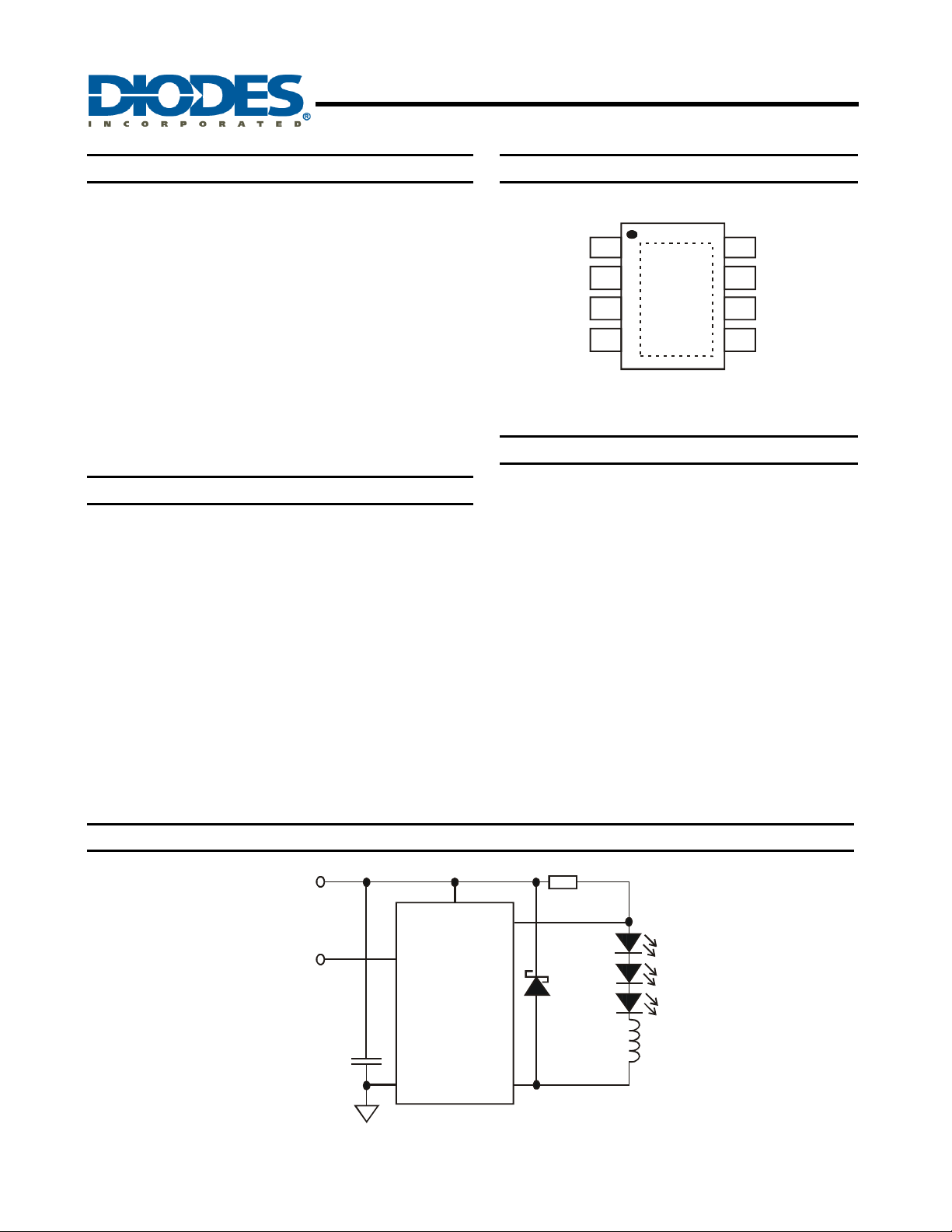
Typical Application Circuit
and SET input pins. Dimming is
IN
60V 1A LED STEP-DOWN CONVERTER
Pin Assignments
(Top View)
SET
GND
NC
V
IN
1
2
3
4
AP8802H
8
7
6
5
CTRL
GND
SW
SW
SO-8EP
Applications
• Commercial & industrial lighting
• Small LCD panel backlight
• Appliances interior lighting
• Architecture Detail lighting
SET
0.33
48V
V
IN
SET
Ω
CTRL
P8802H
D1
PDS3200
L1
C1
2.2µF
AP8802H
Document number: DS32227 Rev. 6 - 2
GND
1 of 14
www.diodes.com
SW
68µF
May 2012
© Diodes Incorporated
Pin Descriptions
Pin Name Function
SW Switch Pin. Connect inductor/freewheeling diode here, minimizing track length at this pin to reduce EMI.
GND GND pin
SET Set Nominal Output Current Pin. Configure the output current of the device.
Dual function dimming control pin with an input impedance approximately 50kΩ.
CTRL
If the CTRL pin is left open then its voltage will default to V
VIN
EP Exposed pad: Internally connected to IC substrate . It should be connected to GND and as large as possible thermal
PRELIMINARY
NEW PRODUCT
NC No connection
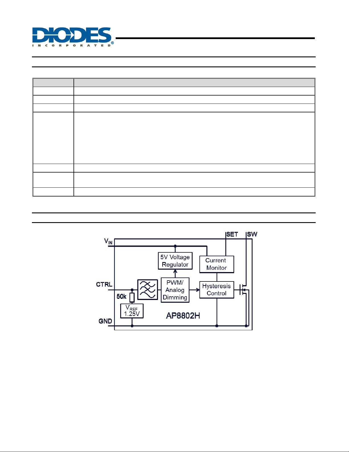
Functional Block Diagram
Input Supply Pin. Must be locally bypassed.
mass for improved thermal impedance and power dissipation capability. See Land Pad diagrams.
AP8802H
60V 1A LED STEP-DOWN CONVERTER
• Input voltage of 0.2V or lower forces the device into low current standby mode and shuts off the output.
• A PWM signal (driven by an open-drain/collector source) allows the output current to be adjusted over a wide
range up to 100%.
• An analog voltage between 0.3V and 2.5V adjusts the output current between 24% and 200% of the current
set by 0.2V/R
.
S
REF
AP8802H
Document number: DS32227 Rev. 6 - 2
Figure. 1 Functional Block Diagram
2 of 14
www.diodes.com
May 2012
© Diodes Incorporated
AP8802H
Absolute Maximum Ratings (Note 4)
Symbol Parameter Rating Unit
VIN VIN pin Voltage
VSW
V
CTRL
V
SENSE
TJ
T
LEAD
T
ST
Note: 4 All voltages unless otherwise stated are measured with respect to GND.
5. V
Caution: Stresses greater than the 'Absolute Maximum Ratings' specified above, may cause permanent damage to the device. These are stress ratings
only; functional operation of the device at conditions between maximum recommended operating conditions and absolute maximum ratings is not
implied. Device reliability may be affected by exposure to absolute maximum rating conditions for extended periods of time.
Semiconductor devices are ESD sensitive and may be damaged by exposure to ESD events. Suitable ESD precautions should be taken when
handling and transporting these devices.
PRELIMINARY
Recommended Operating Conditions
NEW PRODUCT
Symbol Parameter Min Max Unit
VIN
V
CTRLDC
V
CTRLL
f
OSC
TA
Duty Cycle Using Inductor ≥ 100µH (Note 8) 0.10 0.95 —
Notes: 6. For 100% brightness either leave floating or connect to 1.25V relative to GND.
7. AP8802H will operate at higher frequencies but accuracy will be affected due to propagation delays.
8. For most applications the LED current will be within 5% over the duty cycle range specified. Duty cycle accuracy is also dependent on
propagation delay. Smaller size inductors can be used but LED current accuracy may be greater than 8% at extremes of duty cycle. This is most
noticeable at low duty cycles (less than 0.1) or when the input voltage is high and only one LED is being driven.
Electrical Characteristics (V
Symbol Parameter Conditions Min Typ Max Unit
I
OUT
IQ
V
THD
V
SENSEHYS
SET SET pin input current
V
REF
R
DS(ON)
I
SW_LEAKAGE
θ
JA
θ
JC
Notes: 9. Refer to figure 8 for the device derating curve.
10. Test condition for SO-8EP: Device mounted on FR-4 PCB, 2”x2”, 2oz copper, minimum recommended pad layout on top layer and thermal vias to
bottom layer ground plane. See Land pad diagram For better thermal performance, larger copper pad for heat-sink is needed.
SW Voltage -0.3 to +65 V
CTRL Pin Input Voltage -0.3 to +6 V
SET Voltage (Note 5) +0.3 to -5 V
Junction Temperature 150 °C
Lead Temperature Soldering 300 °C
Storage Temperature Range -65 to +150 °C
is measured with respect to V
SENSE
.
IN
Operating Input Voltage relative to GND 8.0 60.0 V
Voltage range for 24% to 200% DC dimming relative to GND (Note 6) 0.3 2.5 V
Voltage Low for PWM dimming relative to GND 0 0.2 V
Maximum Switching Frequency (Note 7) — 625 kHz
Ambient Temperature Range -40 +125 °C
= 12V, TA = +25°C, unless otherwise specified.)
IN
Continuous switch current (Note 9) — — 1 A
Quiescent Current - 75 120 μA
Internal Threshold Voltage 190 200 210 mV
Sense threshold hysteresis — 15 — %
V
SET
Internal Reference Voltage — 1.25 — V
On Resistance of MOSFET
Switch leakage current — - 8 μA
I
SW
= 0.8A
Thermal Resistance Junction-to-Ambient SO-8EP (Note 10) — 45 — °C/W
Thermal Resistance Junction-to-Case SO-8EP (Note 10) — 7 — °C/W
60V 1A LED STEP-DOWN CONVERTER
-0.3 to +65 V
= V
IN
-0.2
— 5 — μA
— 0.65 1.10 Ω
AP8802H
Document number: DS32227 Rev. 6 - 2
3 of 14
www.diodes.com
May 2012
© Diodes Incorporated
O
TCH
G SUPPLY
C
URRENT
CTR
O
T
G
2
CTR
OLTAG
CUR
REN
T
T
C
H
N
G F
R
Q
U
N
C
Y
H
Typical Characteristics
0.9
(mA)
0.8
0.7
AP8802H
60V 1A LED STEP-DOWN CONVERTER
1.256
1.254
0.6
0.5
0.4
IN
0.3
0.2
0.1
N-SWI
N
0
06055510 15 20 25 30 35 40 5045
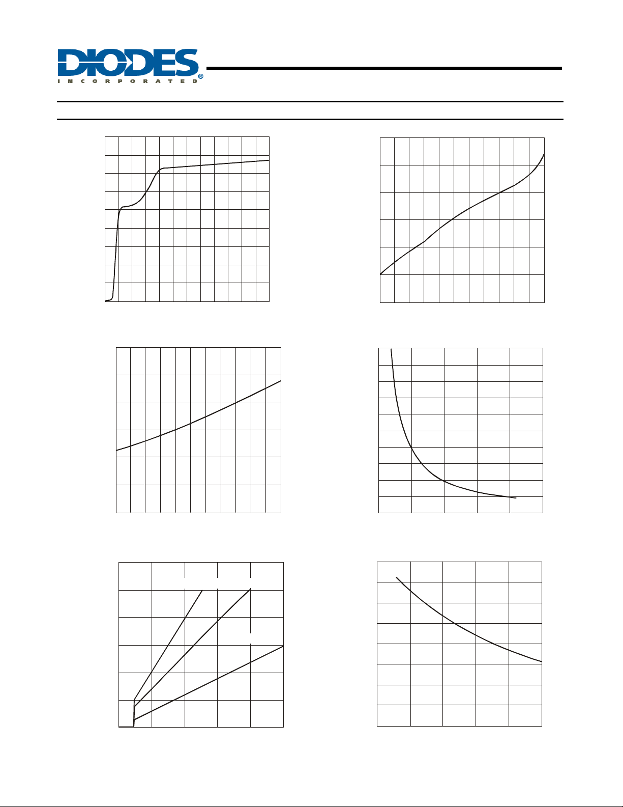
Figure. 2 Supply Current (not switching) vs. Input Voltage
PRELIMINARY
1.
NEW PRODUCT
1.0
0.8
E (V)
0.6
L V
0.4
0.2
0
-40 125-25 110-10 5 20 35 50 65 9580
Figure. 4 R vs. Ambient Temperature
1200
INPUT VOLTAGE (V)
AMBIENT TEMPERATURE (°C)
DS(ON)
1.252
E (V)
A
L
1.250
L V
1.248
1.246
1.244
-40 125-25 110-10 5 20 35 50 65 9580
AMBIENT TEMPERATURE (°C)
1000
(mA)
LED
Figure. 3 V vs. Ambient Temperature
900
800
700
600
500
400
300
200
100
0
0 0.5 1.0 1.5 2.0 2.5
800
CTRL
R RESISTANCE ( )
SET
Figure. 5 LED Current vs. R
Ω
SET
R = 0.3
R = 0.2
Ω
1000
800
600
400
LED CURRENT (mA)
200
0
0 0.5 1.0 1.5 2.0 2.5
Figure. 6 LED Current vs. V
SET
CTRL VOLTAGE (V)
AP8802H
Document number: DS32227 Rev. 6 - 2
SET
R = 0.68
SET
CTRL
Ω
Ω
4 of 14
www.diodes.com
700
z)
(k
600
500
E
E
400
300
I
200
SWI
100
0
02.50.5 1.0 1.5 2.0
Figure. 7 Switching Frequency vs. V
CTRL VOLTAGE (V)
CTRL
May 2012
© Diodes Incorporated
F
FIC
C
Y
TCHIN
G F
REQ
UENCY
H
UTY CYC
Typical Characteristics (T
10
8
6
4
2
0
-2
-4
-6
OUTPUT CURRENT DEVIATION (%)
-8
-10
6 1218 48546024 30 36 42
PRELIMINARY
NEW PRODUCT
z)
(k
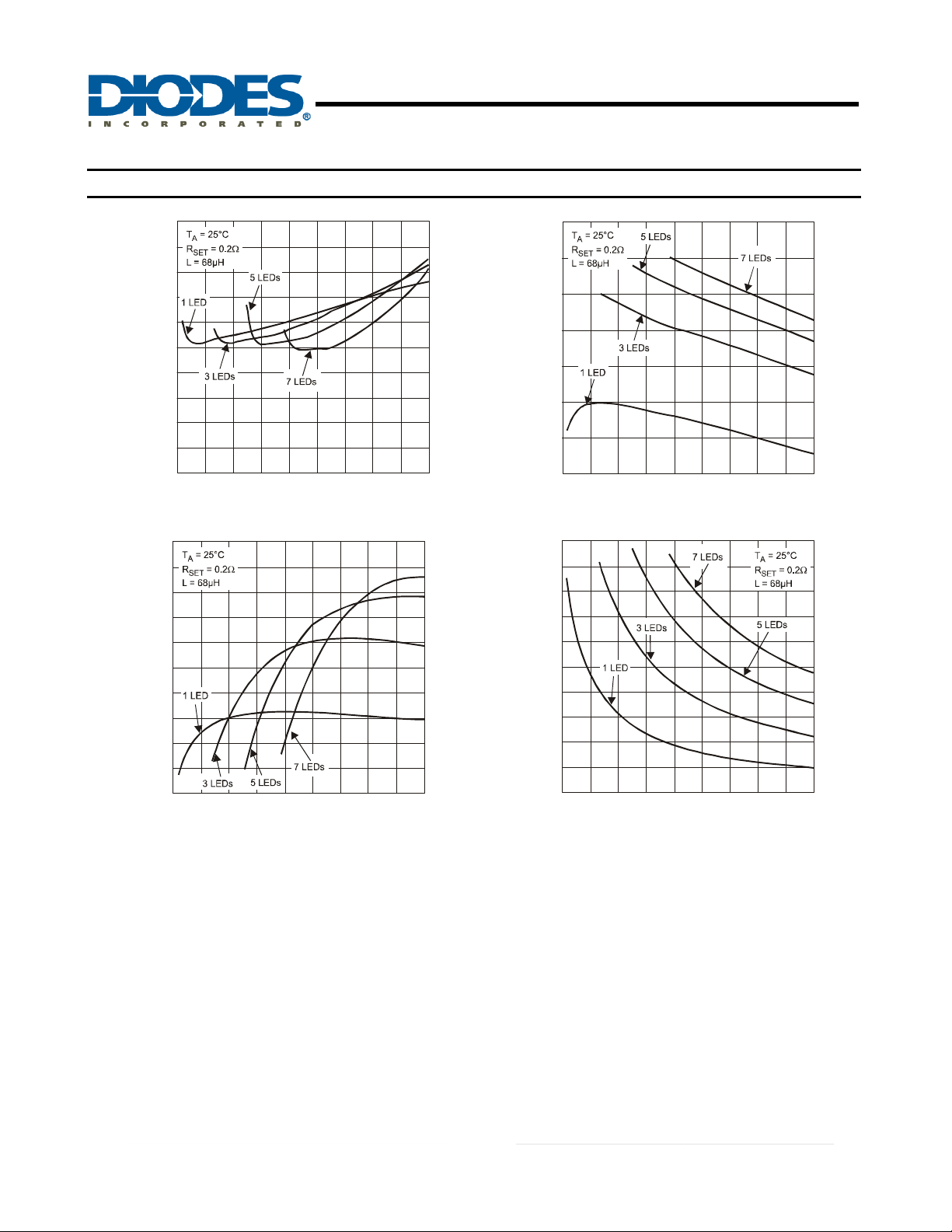
Figure. 8 LED Current vs. Input Voltage
500
450
400
350
= +25°C, VIN = 60V, L = 68µH; unless otherwise stated.)
A
INPUT VOLTAGE (V)
AP8802H
60V 1A LED STEP-DOWN CONVERTER
100
95
90
(%)
85
IEN
80
E
75
70
65
61218 48546024 30 36 42
Figur e. 9 Efficiency vs. Input Voltage
100
90
80
70
INPUT VOLTAGE (V)
300
250
200
150
100
SWI
50
0
6 1218 48546024 30 36 42
Figure. 10 Switching Frequency vs. Input Voltage
INPUT VOLTAGE (V)
60
LE (%)
50
40
D
30
20
10
0
6 1218 48546024 30 36 42
Figure. 11 Duty Cycle vs. Input Voltage
SUPPLY VOLTAGE (V)
Figure. 12 Steady State Waveforms
AP8802H
Document number: DS32227 Rev. 6 - 2
Figure. 13 Start-Up Showing LED Current Soft Start
5 of 14
www.diodes.com
© Diodes Incorporated
May 2012
 Loading...