

Page 1
Description
The AP8801 is a step-down DC/DC converter designed to drive LEDs with
a constant current. The device can drive up to thirteen LEDs, depending on
the forward voltage of the LEDs, in series from a voltage source of 8V to
48V. Series connection of the LEDs provides identical LED currents
resulting in uniform brightness and eliminating the need for ballast
resistors. The AP8801 switches at frequency up to 700kHz. This allows
the use of small size external components, hence minimizing the PCB area
needed.
Maximum output current of AP8801 is set via an external resistor
connected between the V
applying either a DC voltage or a PWM signal at the CTRL input pin. An
input voltage of 0.2V or lower at CTRL shuts down the output at SW and
puts the device into a low-current standby state.
Features
• LED driving current up to 500mA
• Operating input voltage up to 48V
• High efficiency up to 92%
• High switching frequency up to 700kHz
• PWM/DC input for dimming control
• Built-in output open-circuit protection
• SO-8 and MSOP-8 are in “Green” Molding Compound (No Br, Sb)
Totally Lead-Free & Fully RoHS Compliant (Notes 1 & 2)
Halogen and Antimony Free. “Green” Device (Note 3)
and SET input pins. Dimming is achieved by
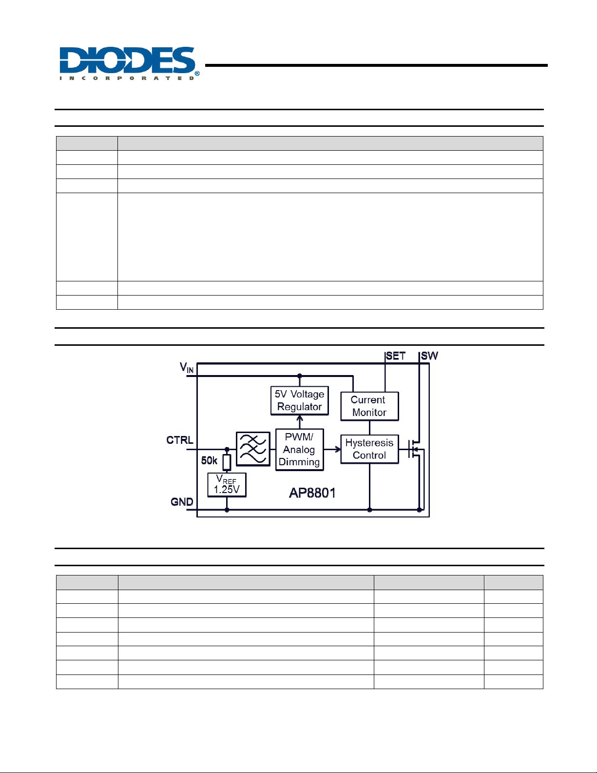
IN
AP8801
500mA LED STEP-DOWN CONVERTER
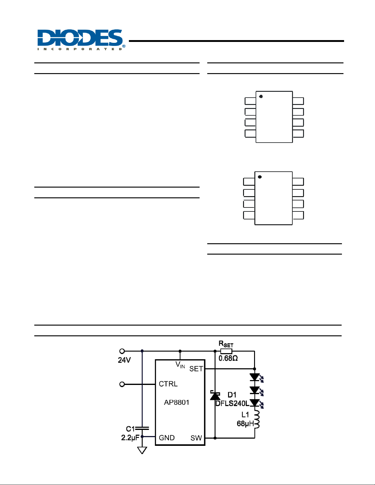
Pin Assignments
SET
GND GND
NC
V
IN
SET
GND GND
NC
V
IN
Applications
• Commercial & industrial lighting
• Small LCD panel backlight
• Appliances interior lighting
• Architecture Detail lighting
(Top View)
1
2
AP8801
3
45
SO-8
8
7
6
CTRL
SW
SW
(Top View)
1
2
AP8801
3
45
MSOP-8
8
7
6
CTRL
SW
SW
Notes: 1. No purposely added lead. Fully EU Directive 2002/95/EC (RoHS) & 2011/65/EU (RoHS 2) compliant.
2. See http://www.diodes.com for more information about Diodes Incorporated’s definitions of Halogen- and Antimony-free, "Green" and Lead-free.
3. Halogen- and Antimony-free "Green” products are defined as those which contain <900ppm bromine, <900ppm chlorine (<1500ppm total Br + Cl)
and <1000ppm antimony compounds.
Typical Application Circuit
June 2012
© Diodes Incorporated
AP8801
Document number: DS31765 Rev. 7 - 2
1 of 14
www.diodes.com
Page 2
500mA LED STEP-DOWN CONVERTER
Pin Descriptions
Pin Name Functions
SW Switch Pin. Connect inductor/freewheeling diode here, minimizing track length at this pin to reduce EMI.
GND GND pin
SET Set Nominal Output Current Pin. Configure the output current of the device.
Dual Function Dimming Control Pin.
• Input voltage of 0.2V or lower forces the device into low current standby mode and shuts off the output.
• A PWM signal (driven by an open-drain/collector source) allows the output current to be adjusted over a wide
CTRL
The input impedance is about 50kΩ, and if the pin is left open V
VIN
NC No connection
Input Supply Pin. Must be locally bypassed.
range up to 100%.
• An analog voltage between 0.3V and 2.5V adjusts the output current between 25% and 200% of the current set
by 0.2V/R
.
S
= V
CTRL
REF
Functional Block Diagram
AP8801
Fig. 1 Block Diagram
Absolute Maximum Ratings
Symbol Parameter Rating Unit
VIN VIN pin voltage
VSW
V
CTRL
V
SENSE
TJ
T
LEAD
T
ST
Caution: Stresses greater than the 'Absolute Maximum Ratings' specified above, may cause permanent damage to the device. These are stress ratings only;
functional operation of the device at these or any other conditions exceeding those indicated in this specification is not implied. Device reliability may
be affected by exposure to absolute maximum rating conditions for extended periods of time.
Semiconductor devices are ESD sensitive and may be damaged by exposure to ESD events. Suitable ESD precautions should be taken when
handling and transporting these devices.
AP8801
Document number: DS31765 Rev. 7 - 2
SW voltage -0.3 to +50 V
CTRL Pin Input Voltage -0.3 to +6 V
SET Voltage +0.3 to -5 V
Junction Temperature 150
Lead Temperature Soldering 300
Storage Temperature Range -65 to +150
2 of 14
www.diodes.com
-0.3 to +50 V
o
o
o
June 2012
© Diodes Incorporated
C
C
C
Page 3
AP8801
500mA LED STEP-DOWN CONVERTER
Recommended Operating Conditions
Symbol Parameter Min Max Unit
VIN
V
CTRLDC
V
CTRLL
f
OSC
TA
Duty Cycle Using Inductor ≥ 100µH (Note 6) 0.10 0.95 —
Notes: 4. For 100% brightness either leave floating or connect to 1.25V relative to GND.
5. AP8801 will operate at higher frequencies but accuracy will be affected due to propagation delays.
6. For most applications the LED current will be within 8% over the duty cycle range specified. Duty cycle accuracy is also dependent on
propagation delay. Smaller size inductors can be used but LED current accuracy may be greater than 8% at extremes of duty cycle. This is most
noticeable at low duty cycles (less than 0.1) or when the input voltage is high and only one LED is being driven.
Electrical Characteristics (T
Symbol Parameter Conditions Min Typ Max Unit
I
OUT
IQ
V
THD
V
SENSEHYS
V
REF
SET SET pin input current
R
DS(ON)
I
SW_LEAKAGE
θ
JA
θ
JC
Notes: 7. Refer to figure 6 for the device derating curve.
8. Test condition for SO-8 and MSOP-8: Device mounted on FR-4 PCB, 2”x2”, 2oz copper, minimum recommended pad layout on top layer and
thermal vias to bottom layer ground plane. For better thermal performance, larger copper pad for heat-sink is needed.
AP8801
Document number: DS31765 Rev. 7 - 2
Operating Input Voltage relative to GND 8.0 48.0 V
Voltage range for 24% to 200% DC dimming relative to GND (Note 4) 0.3 2.5 V
Voltage Low for PWM dimming relative to GND 0 0.2 V
Maximum Switching Frequency (Note 5) — 625 kHz
Ambient Temperature Range -40 +105 ºC
= 25°C, VIN = 24V; unless otherwise specified.)
A
Continuous switch current (Note 7) — — 500 mA
Quiescent Current — 78 120 μA
Internal Threshold Voltage 184 200 216 mV
Sense threshold hysteresis — 15 — %
Internal Reference Voltage — 1.25 — V
V
= V
IN
= 0.4A
-0.2
SET
On Resistance of MOSFET
Switch leakage current — — 8 μA
Thermal Resistance Junction-to-Ambient
Thermal Resistance Junction-to-Case
I
SW
SO-8 (Note 8) — 88 — °C/W
MSOP-8 (Note 8) — 128 — °C/W
SO-8 (Note 8) — 58 — °C/W
MSOP-8 (Note 8) — 90 — °C/W
3 of 14
www.diodes.com
— 7 — μA
— 0.70 1.15 Ω
June 2012
© Diodes Incorporated
Page 4
NON
T
C
HIN
G SUPPLY CUR
REN
T
CTR
OLTAG
R
CUR
REN
T
C
URRENT
TCH
N
G
F
R
Q
U
N
C
Y
H
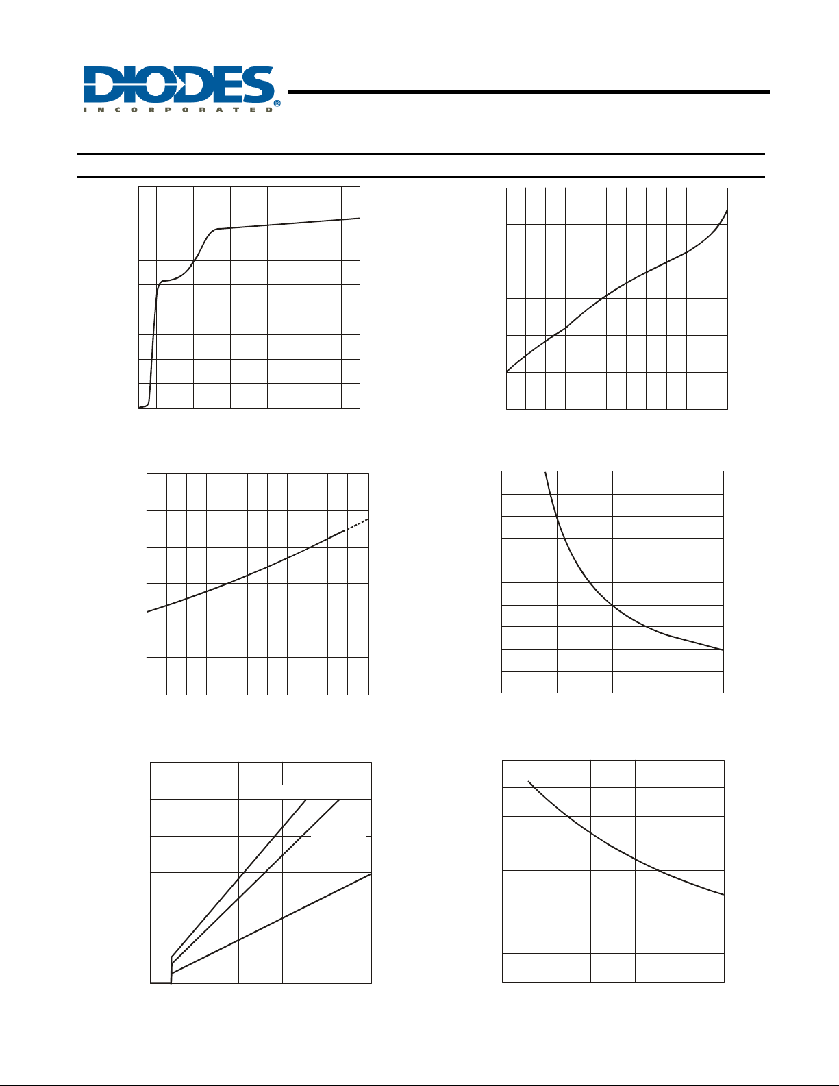
Typical Characteristics
0.9
(mA)
0.8
0.7
AP8801
500mA LED STEP-DOWN CONVERTER
1.256
1.254
0.6
0.5
0.4
0.3
0.2
-SWI
0.1
0
06055510 15 20 25 30 35 40 5045
Figure. 2 Supply Current (not switching) vs. Input Voltage
1.2
1.0
0.8
Ω
()
0.6
DS(ON)
0.4
0.2
0
-40 -25 -10 5 20 35 50 65 80 95 110 125
600
INPUT VOLTAGE (V)
AMBIENT TEMPERATURE (C)
Figure. 4 R vs Ambient Temperature
DS(ON)
1.252
E (V)
1.250
L V
1.248
1.246
1.244
-40 125-25 110-10 5 20 35 50 65 9580
AMBIENT TEMPERATURE (°C)
500
450
400
350
(mA)
300
250
200
LED
150
100
Figure. 3 V vs. Ambient Temperature
50
0
0 0.5 1.5 2.01.0
800
CTRL
R RESISTANCE ( )
SET
Figure. 5 LED Current vs. R
Ω
SET
500
400
(mA)
300
200
LED
100
0
02.50.5 1.0 1.5 2.0
Figure. 6 LED Current vs. V
R = 0.56
CTRL VOLTAGE (V)
AP8801
Document number: DS31765 Rev. 7 - 2
SET
Ω
R = 0.68
SET
R = 1.33
SET
CTRL
Ω
Ω
4 of 14
www.diodes.com
700
z)
(k
600
500
E
E
400
300
I
200
SWI
100
0
02.50.5 1.0 1.5 2.0
Figure. 7 Switching Frequency vs. V
CTRL VOLTAGE (V)
CTRL
June 2012
© Diodes Incorporated
Page 5
F
FIC
C
Y
UTY CYC
Typical Characteristics (T
10
8
6
4
2
0
-2
-4
-6
OUTPUT CURRENT DEVIATION (%)
-8
-10
61218 4824 30 36 42
SUPPLY VOLTAGE (V)
Figure . 8 LED Current vs. In put Volt age
700
600
500
500mA LED STEP-DOWN CONVERTER
= +25°C, VIN = 60V, L =68µH unless otherwise stated.)
A
100
95
90
85
(%)
80
75
IEN
70
E
65
60
55
50
61218 4824 30 36 42
SUPPLY VOLTAGE (V)
100
90
80
70
Figure. 9 Efficiency vs. Input Voltage
AP8801
400
300
200
100
SWITCHING FREQUENCY (kHz)
0
61218 4824 30 36 42
Figure. 10 Sw i tching Frequency vs. Input Voltage
SUPPLY VOLTAGE (V)
60
LE (%)
50
40
D
30
20
10
0
61218 4824 30 36 42
SUPPLY VOLTAGE (V)
Figure. 11 Duty Cycle vs. Input Voltage
Figure. 12 Steady State Waveforms
AP8801
Document number: DS31765 Rev. 7 - 2
5 of 14
www.diodes.com
Figure.13 Start-Up Showing LED Current Soft -Start
June 2012
© Diodes Incorporated
Page 6

REQ
U
C
Y
H
Application Information
LED Current Control
The LED current is controlled by the resistor R
LED(s) is defined as:
V
I = where V
LED
THD
R
SET
AP8801
500mA LED STEP-DOWN CONVERTER
in Figure 14 connected between VIN and SET. The nominal average output current in the
SET
is the voltage between the VIN and SET pins and is nominally 200mV.
THD
Figure. 14 Typical Application Circuit for I
LED
= 0.3A
Inductor Selection
This section highlights how to select the inductor suitable for the application requirements in terms of switching frequency, LED current
accuracy and temperature.
AP8801
Document number: DS31765 Rev. 7 - 2
600
47
47
0
0 50 100 150 200 250 300 400 450 500350
z)
(k
EN
F
500
400
300
200
100
100
68
150
100
150
68
100
150
INDUCTOR VALUE (µH)
Figure. 15 Switching Frequency vs. Inductor Value
220
220
220
6 of 14
www.diodes.com
Switching Frequency @I = 500mA
LED
12V - 1 LED
24V - 3 LEDs
48V - 6 LEDs
470
470
470
© Diodes Incorporated
June 2012
Page 7

AP8801
Application Information (cont.)
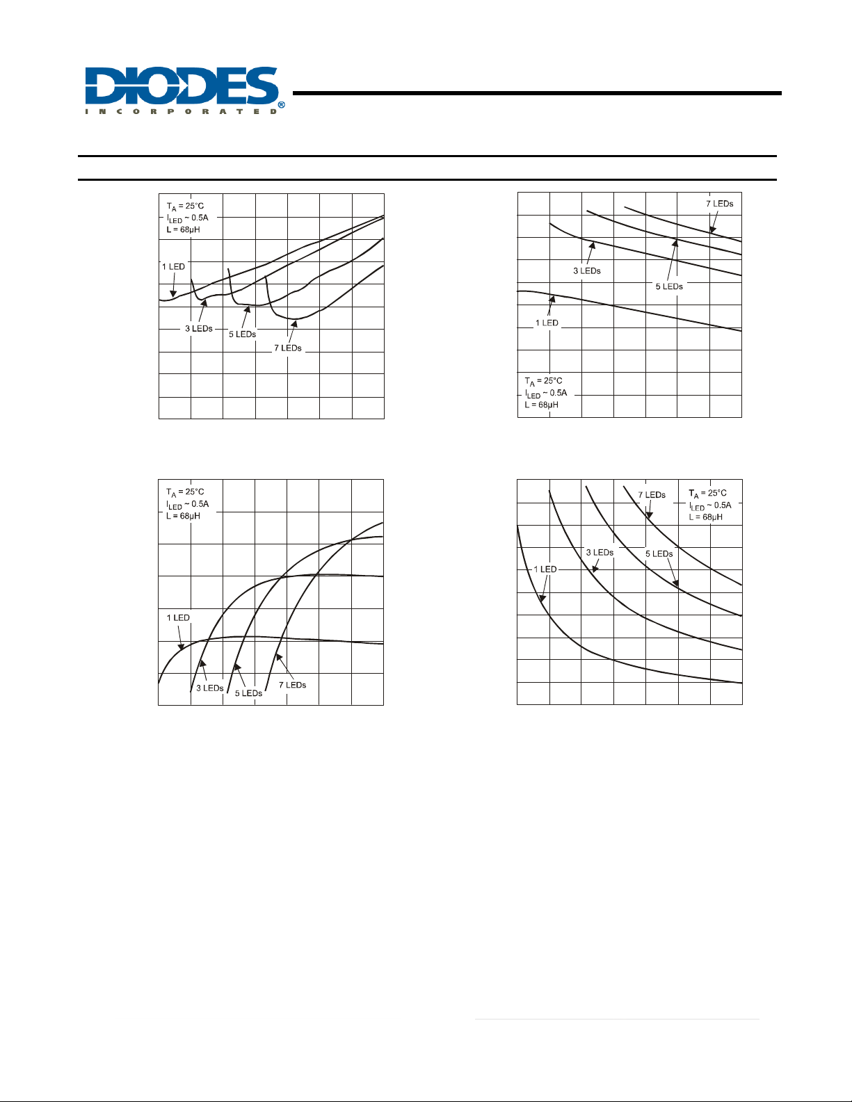
The inductor influences the LED current accuracy that the system is able to provide. The following section highlights how to select the
inductor in relation to the device packages and the LED current, while maintaining the chip temperature below 70°C.
12
11
10
47µH
68µH
100µH
150µH
220µH
9
8
470µH
8% Accuracy, <70°C Case Temperature
500mA LED STEP-DOWN CONVERTER
7
6
NUMBER of LEDs
5
4
3
2
1
0 5 10 15 30 35 40 4520 25
Figure. 16 Minimum Recommended Inductor with 500mA LED Current
47µH
SUPPLY VOLTAGE (V)
100µH
68µH
220µH
150µH
470µH
Capacitor Selection
The small size of ceramic capacitors makes them ideal for AP8801 applications. X5R and X7R types are recommended because they retain
their capacitance over wider voltage and temperature ranges than other types such as Z5U. A 2.2μF input capacitor is sufficient for most
intended applications of AP8801.
A 4.7μF input capacitor is suggested for application with an input voltage equal or higher than 40V.
Diode Selection
Schottky diodes, e.g. B1100, with their low forward voltage drop and fast reverse recovery, are the ideal choice for AP8801 applications.
AP8801
Document number: DS31765 Rev. 7 - 2
7 of 14
www.diodes.com
June 2012
© Diodes Incorporated
Page 8

AP8801
CUR
RENT
Application Information (cont.)
LED Current Adjustment/Dimming.
The LED current for the AP8801 can be adjusted by driving the CTRL with a digital signal (PWM dimming) or by driving the CTRL with a dc
voltage between 0.3V and 2.5V (DC dimming).
If the CTRL pin is driven by an external voltage (lower than 2.5V), the average LED current is:
V
I ×=
LED
V
600
500
0.4
0.47
400
(mA)
300
LED
200
100
0.56
0.68
0.47
0.68
0
0 0.3 0.6 0.9 1.2 1.5 1.8 2.4 2.7 32.1
Figure. 17 LED Current vs. R and V
Figure 17 shows that reducing the CTRL voltage by a factor of 2 also reduces the LED curr ent by a factor of 2. The AP8801 has the ability
vary the LED current by a factor of 2 above the default value set by RSET down to a factor of 0.24 of the nominal LED current. This pro vides
an 8.33:1 dynamic range of the dc dimming.
A low pass filter on the CTRL pin of the AP8801 automatically provides some soft-start function of the LED current on initial start-up (this
phenomenon can be seen in figure 7); the built in soft-start period can be increased by the addition of an external capacitor onto the CTRL
pin.
The AP8801’s dimming range can be increased above this dc dimming factor by applying a PWM signal to the CTRL pin using this method
dimming dynamic ranges above 100 can be achieved.
AP8801
Document number: DS31765 Rev. 7 - 2
V
CTRL
REF
0.82
THD
R
0.82
1
0.82
1
1
www.diodes.com
where V
SET
1.2
1.2
1.2
R VALUE ()
SET
8 of 14
500mA LED STEP-DOWN CONVERTER
is nominally 1.25V
REF
LED Current @
V = 1.25V
CTRL
LED Current @
V = 2.5V
CTRL
LED Current @
V = 0.625V
CTRL
1.5
2
1.5
2
1.5
2
Ω
SET CTRL
3
3
3
© Diodes Incorporated
June 2012
Page 9

AP8801
Application Information (cont.)
PWM Dimming of LED Current
When a low frequency PWM signal with voltages between 2.5V and a low level of zero is applied to the CTRL pin the output current will be
switched on and off at the PWM frequency. The resultant LED current I
A Pulse Width Modulated (PWM) signal with a max resolution of 8-bit, can be applied to the CTRL pin to change the output current to a value
above or below the nominal average value set by resistor R
To achieve this resolution the PWM frequency has to be lower than 500Hz. The ultimate resolution will be determined by the number of
switching cycles required to get back to nominal LED current once the PWM voltage is high relative to PWM frequency. Lower switching
frequencies and higher PWM frequencies will result in lower PWM dimming dynamic ranges.
SET
LEDavg
.
500mA LED STEP-DOWN CONVERTER
will be proportional to the PWM duty cycle. See figure 18.
Figure. 18 Low Frequency PWM Operating Waveforms
There are different ways of accomplishing PWM dimming of the AP8801 LED current:
Directly Driving CTRL Input
A Pulse Width Modulated (PWM) signal with duty cycle DPWM can be applied to the CTRL pin to adjust the output current to a value above
or below the nominal average value set by resistor R
exceed a drive voltage of 2.5V (where extra brightness is required) or 1.25V if a maximum of 100% brightness is required.
A way of avoiding over-driving the CTRL pin is use an open collector/drain driver to drive the CTRL pin.
. When driving the CTRL with a voltage waveform care should be taken not to
SET
Driving the CTRL Input via Open Collector Transistor
The recommended method of driving the CTRL pin and controlling the amplitude of the PWM waveform is to use a small NPN s witching
transistor. This uses the internal pull-up resistor between the CTRL pin and the internal voltage reference to pull-up CTRL pin when the
external transistor is turned off.
Driving the CTRL Input from a Microcontroller
If the CTRL pin is driven by a MOSFET (either discrete or open-drain output of a micro-controller) then Schottky diode maybe be required
due to high Gate / Drain capacitance, which could inject a negative spike into CTRL input of the AP8801 and cause erratic operation but the
addition of a Schottky clamp diode (eg. Diodes Inc. SD103CWS) to ground and inclusion of a series resistor (3.3k) will prevent this.
AP8801
Document number: DS31765 Rev. 7 - 2
9 of 14
www.diodes.com
June 2012
© Diodes Incorporated
Page 10

AP8801
d
OFT-STAR
T T
P
O
R
PATIO
Application Information (cont.)
Soft-Start
An external capacitor from the CTRL pin to ground will provide a soft-start delay, by increasing the time taken for the voltage on this pin to
rise to the turn-on threshold and by slowing down the rate of rise of the control voltage at the input of the comparator. Adding capacitance
increases this delay by approximately 200µs/nF. The graph below shows the variation of soft-start time for different values of capacitor.
16
14
12
10
IME ( ms)
8
6
4
S
2
500mA LED STEP-DOWN CONVERTER
0
-2
020406080100120
Figure. 19 Soft-Start Time vs. Capacitance
CAPACITANCE (nf)
from ADJ Pin to Groun
Thermal Considerations
The graph below in figure 20, gives details for power derating. This assumes the d evice to be on a FR-4 PCB, 2”x2”, 2oz copper, mi nimum
recommended pad layout on top layer and thermal vias to bottom layer ground plane standing in still air.
1.2
1.0
N (W)
0.8
MSOP-8
0.6
DISSI
0.4
WE
0.2
SO-8
0
-50 -25 0 50 75 100 125
AMBIENT TEMPERATURE (°C)
Figure. 20 Maximum Power Dissipation
AP8801
Document number: DS31765 Rev. 7 - 2
25
10 of 14
www.diodes.com
June 2012
© Diodes Incorporated
Page 11

AP8801
Application Information (cont.)
Package Selection
The device comes with a wide selection of packages. The suggested package is able to provide a case temperature below 70˚C (with an
ambient temperature of +25°C) for the combination of input voltage and load requested.
12 LEDs
10 LEDs
8 LEDs
I = 500mA
LED
L = 100µH
500mA LED STEP-DOWN CONVERTER
6 LEDs
4 LEDs
2 LEDs
MSOP-8
SO-8
812162024 28 32 36 40 44 48
Figure. 21 Package Section
SO-8
Fault Condition Operation
The AP8801 has by default open LED protection. If the LEDs should become open circuit the AP8801 will stop oscillating; the SET pin will
rise to V
If the LEDs should become shorted together the AP8802H will continue to switch however the duty cycle at which it will operate will change
dramatically and the switching frequency will most likely decrease. The on-time of the internal power MOSFET switch will be significantly
reduced because almost all of the input voltage is now developed across the inductor. The off-time will be significantly increased because the
reverse voltage across the inductor is now just the Schottky diode voltage (See Figure 20) causing a much slower decay in inductor c urrent.
During this condition the inductor current will remain within its controlled levels and so no excessive heat will be generated within the
AP8801.
and the SW pin will then fall to GND. No excessive voltages will be seen by the AP8801.
IN
AP8801
Document number: DS31765 Rev. 7 - 2
Figure. 22 Switching Characteristics
(normal open to short LED chain)
11 of 14
www.diodes.com
June 2012
© Diodes Incorporated
Page 12

X
Ordering Information
500mA LED STEP-DOWN CONVERTER
AP8801 -
Package Green Packing
XG 13
AP8801
G : GreenS : SO-8
M8 : MSOP-8
Device Package Code
AP8801SG-13 S SO-8 2500/Tape & Reel -13
AP8801M8G-13 M8 MSOP-8 2500/Tape & Reel -13
Note: 9. Pad layout as shown on Diodes Inc. suggested pad layout document AP02001, which can be found on our website at
http://www.diodes.com/datasheets/ap02001.pdf.
Packaging
(Note 9)
13 : Tape & Reel
13” Tape and Reel
Quantity Part Number Suffix
Marking Information
(1) SO-8
( Top View )
5
G : Green
YY
: Year : 08, 09,10~
X
41
WW : Week : 01~52; 52
represents 52 and 53 week
: Internal Code
X
(2) MSOP-8
Logo
Part Number
8
AP8801
WW X
YY
( Top View )
Part Number
AP8801
Document number: DS31765 Rev. 7 - 2
Logo
8765
Y W X
AP8801
234
1
12 of 14
www.diodes.com
A~Z : Green
: Year : 0~9
Y
: Week : A~Z : 1~26 week;
W
a~z : 27~52 week; z represents
52 and 53 week
June 2012
© Diodes Incorporated
Page 13

Package Outline Dimensions
(1) SO-8
(2) MSOP-8
AP8801
Document number: DS31765 Rev. 7 - 2
A2
A1
E1
E
A2
A3
A
e
x
y
1
b
D
D
0.25
E
Gauge Plane
Seating Plane
b
A3
A
e
A1
AP8801
500mA LED STEP-DOWN CONVERTER
Dim Min Max
0.254
Gaug e Plan e
Seating Plane
L
Detail ‘A’
7°~9
h
°
45
4
x
1
0
°
4
L
x
1
0
°
Detail C
E3
E1
See Detail C
www.diodes.com
°
Detail ‘A’
Dim Min Max Typ
A1 0.05 0.15 0.10
A2 0.75 0.95 0.86
A3 0.29 0.49 0.39
a
E1 2.90 3.10 3.00
E3 2.85 3.05 2.95
c
All Dimensions in mm
13 of 14
SO-8
A - 1.75
A1 0.10 0.20
A2 1.30 1.50
A3 0.15 0.25
b 0.3 0.5
D 4.85 4.95
E 5.90 6.10
E1 3.85 3.95
e 1.27 Typ
h - 0.35
L 0.62 0.82
0° 8°
θ
All Dimensions in mm
MSOP-8
A - 1.10 -
b 0.22 0.38 0.30
c 0.08 0.23 0.15
D 2.90 3.10 3.00
E 4.70 5.10 4.90
e - - 0.65
L 0.40 0.80 0.60
a 0° 8° 4°
x - - 0.750
y - - 0.750
© Diodes Incorporated
June 2012
Page 14

AP8801
500mA LED STEP-DOWN CONVERTER
IMPORTANT NOTICE
DIODES INCORPORATED MAKES NO WARRANTY OF ANY KIND, EXPRESS OR IMPLIED, WITH REGARDS TO THIS
DOCUMENT, INCLUDING, BUT NOT LIMITED TO, THE IMPLIED WARRANTIES OF MERCHANTABILITY AND FITNESS FOR A
PARTICULAR PURPOSE (AND THEIR EQUIVALENTS UNDER THE LAWS OF ANY JURISDICTION).
Diodes Incorporated and its subsidiaries reserve the right to make modifications, enhancements, improvements, corrections or other
changes without further notice to this document and any product described herein. Diodes Incorporated does not assume any liability
arising out of the application or use of this document or any product described herein; neither does Diodes Incorporated convey any
license under its patent or trademark rights, nor the rights of others. Any Customer or user of this document or products described
herein in such applications shall assume all risks of such use and will agree to hold Diodes Incorporated and all the companies
whose products are represented on Diodes Incorporated website, harmless against all damages.
Diodes Incorporated does not warrant or accept any liability whatsoever in respect of any products purchased through unauthorized
sales channel.
Should Customers purchase or use Diodes Incorporated products for any unintended or unauthorized application, Customers shall
indemnify and hold Diodes Incorporated and its representatives harmless against all claims, damages, expenses, and attorney fees
arising out of, directly or indirectly, any claim of personal injury or death associated with such unintended or unauthorized application.
Products described herein may be covered by one or more United States, international or foreign patents pending. Product names
and markings noted herein may also be covered by one or more United States, international or foreign trademarks.
LIFE SUPPORT
Diodes Incorporated products are specifically not authorized for use as critical components in life support devices or systems without
the express written approval of the Chief Executive Officer of Diodes Incorporated. As used herein:
A. Life support devices or systems are devices or systems which:
1. are intended to implant into the body, or
2. support or sustain life and whose failure to perform when properly used in accordance with instructions for use provided
in the labeling can be reasonably expected to result in significant injury to the user.
B. A critical component is any component in a life support device or system whose failure to perform can be reasonably expected
to cause the failure of the life support device or to affect its safety or effectiveness.
Customers represent that they have all necessary expertise in the safety and regulatory ramifications of their life support devices or
systems, and acknowledge and agree that they are solely responsible for all legal, regulatory and safety-related requirements
concerning their products and any use of Diodes Incorporated products in such safety-critical, life support devices or systems,
notwithstanding any devices- or systems-related information or support that may be provided by Diodes Incorporated. Further,
Customers must fully indemnify Diodes Incorporated and its representatives against any damages arising out of the use of Diodes
Incorporated products in such safety-critical, life support devices or systems.
Copyright © 2012, Diodes Incorporated
www.diodes.com
AP8801
Document number: DS31765 Rev. 7 - 2
14 of 14
www.diodes.com
June 2012
© Diodes Incorporated
 Loading...