

Page 1
Dual 1A, 1.5MHZ Synchronous Step-down DC-DC Converter AP3427M
Preliminary Datasheet
General Description
The AP3427M is a high efficiency step-down dual
channel DC-DC voltage converter. The chip
operation is optimized by peak-current mode
architecture with built-in synchronous power
MOSFET switchers. The oscillator and timing
capacitors are all built-in providing an internal
switching frequency of 1.5MHz that allows the use of
small surface mount inductors and capacitors for
portable product implementations.
Integrated Soft Start (SS), Under Voltage Lock Out
(UVLO), Thermal Shutdown Detection (TSD) and
Short Circuit Protection are designed to provide
reliable product applications.
The device is available in adjustable output voltage
ranging from 0.6V to 0.9×V
range is from 2.5V to 5.5V, and is able to deliver up
to 1A.
The AP3427M is available in standard DFN-3×3-10
package.
when input voltage
IN
Features
• High Efficiency Buck Power Converter
• Output Current: 1.0A
• Low R
• Adjustable Output Voltage from 0.6V to 0.9×V
• Wide Operating Voltage Range: 2.5V to 5.5V
• Built-in Power Switches for Synchronous
Rectification with High Efficiency
• Feedback Voltage: 600mV
• 1.5MHz Constant Frequency Operation
• Thermal Shutdown Protection
• Low Drop-out Operation at 100% Duty Cycle
• Input Over Voltage Protection
• No Schottky Diode Required
Internal Switches:200mΩ (VIN=5V)
DS(ON)
Applications
• Post DC-DC Voltage Regulation
• PDA and Notebook Computer
DFN-3×3-10
Figure 1. Package Type of AP3427M
IN
Mar. 2013 Rev. 1.0 BCD Semiconductor Manufacturing Limited
1
Page 2
Preliminary Datasheet
Dual 1A, 1.5MHZ Synchronous Step-down DC-DC Converter AP3427M
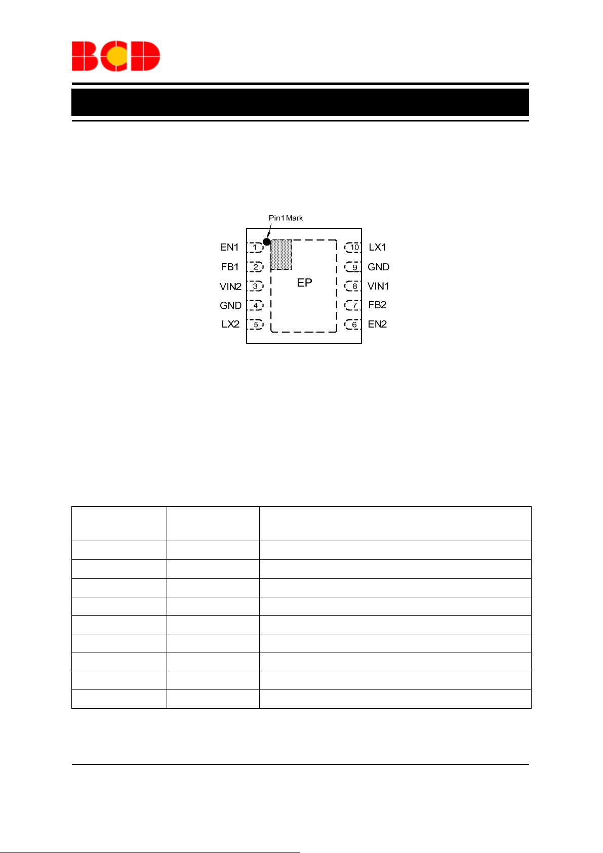
Pin Configuration
DN Package
(DFN-3×3-10)
Figure 2. Pin Configuration of AP3427M (Top View)
Pin Description
Pin Number Pin Name Function
1 EN1 Enable signal input of channel 1, active high
2 FB1 Feedback voltage of channel 1
3 VIN2 Power supply input of channel 2
4, 9, Exposed Pad GND GND. It should be connected to system ground
5 LX2 Connected from channel 2’s Power MOSFET to inductor
6 EN2 Enable signal input of channel 2, active high
7 FB2 Feedback voltage of channel 2
8 VIN1 Power supply input of channel 1
10 LX1 Connected from channel 1’s Power MOSFET to inductor
Mar. 2013 Rev. 1.0 BCD Semiconductor Manufacturing Limited
2
Page 3
Preliminary Datasheet
Dual 1A, 1.5MHZ Synchronous Step-down DC-DC Converter AP3427M
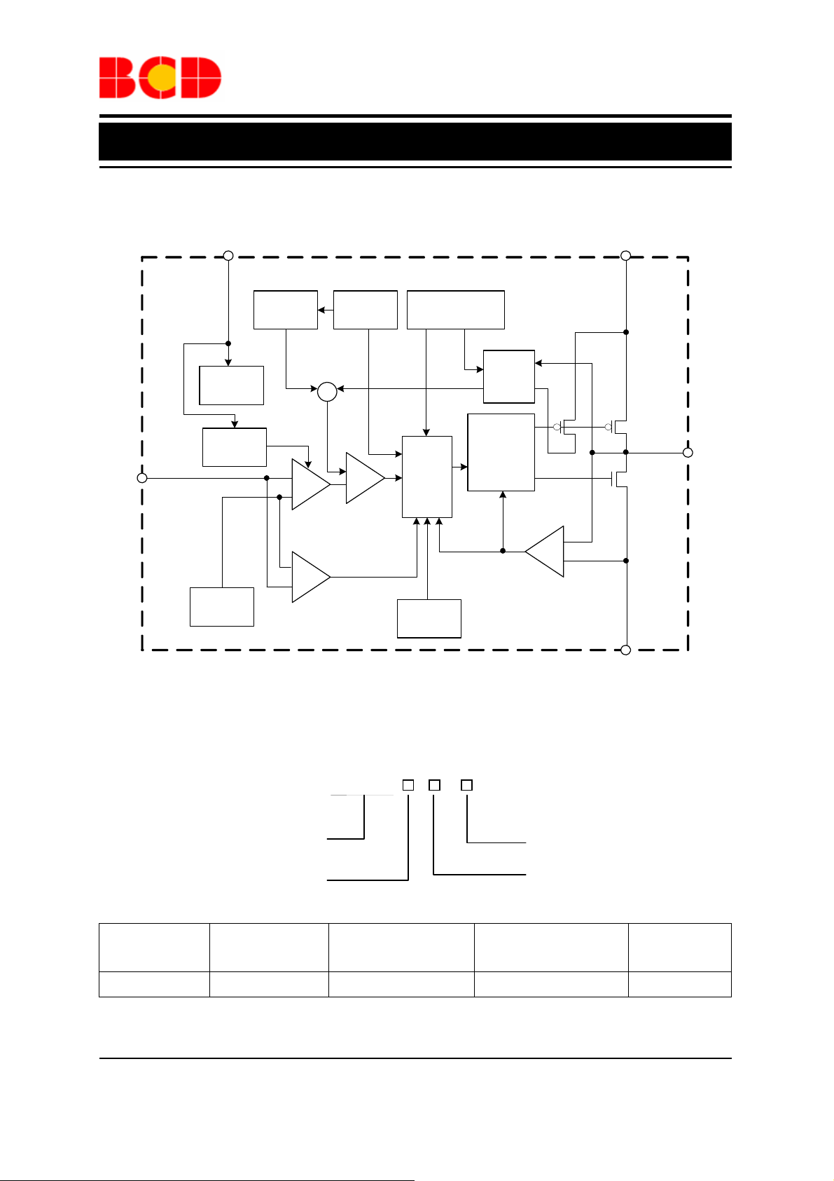
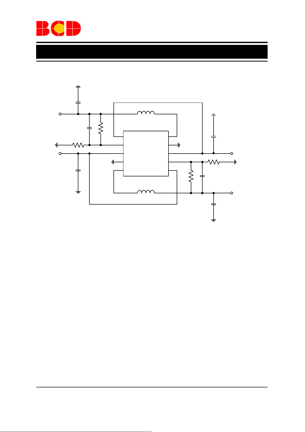
Functional Block Diagram
FB1/
FB2
2/7
EN 1/EN2
1/6 8/3
Over Current
Comparator
Control
Logic
Reverse Inductor
Current Comparator
Thermal
Shutdown
Current
Sensing
Buffer &
Dead Time
Control
Logic
Bias
Generator
Soft
Start
Bandgap
Reference
Saw-tooth
Generator
-
+
Error
Amplifier
-
+
Oscillator
+
+
-
Modulator
Over Voltage
Comparator
VIN1/VIN2
-
+
4/9
10/5
LX1/
LX2
GND
Figure 3. Functional Block Diagram of AP3427M
Ordering Information
AP3427M -
Circuit Type G1: Green
Package
DN: DFN-3×3-10
Package
DFN-3×3-10
Temperature
Range
-40 to 80°C
Part Number Marking ID
AP3427MDNTR-G1 BFE Tape & Reel
BCD Semiconductor's Pb-free products, as designated with "G1" suffix in the part number, are RoHS compliant
and green.
Mar. 2013 Rev. 1.0 BCD Semiconductor Manufacturing Limited
3
TR: Tape & Reel
Packing
Type
Page 4
Preliminary Datasheet
Dual 1A, 1.5MHZ Synchronous Step-down DC-DC Converter AP3427M
Absolute Maximum Ratings (Note 1)
Parameter Symbol Value Unit
Supply Input Voltage for the
MOSFET Switch
LX Pin Switch Voltage V
Enable Input Voltage V
LX Pin Switch Current I
Power Dissipation (on PCB,
=25°C)
T
A
Thermal Resistance (Junction to
Ambient, Simulation)
Thermal Resistance (Junction to
Case, Simulation)
Operating Junction Temperature TJ 155
, V
V
IN1
LX1
EN1
LX1
0 to 6.5 V
IN2
, V
-0.3 to VIN+0.3 V
LX2
, V
-0.3 to VIN+0.3 V
EN2
, I
1.8 A
LX2
2.44 W
P
D
θ
JA
θ
JC
41
4.2
°C/W
°C/W
°C
Operating Temperature TOP -40 to 85
Storage Temperature Range T
ESD (Human Body Model) V
ESD (Machine Model)
Note 1: Stresses greater than those listed under “Absolute Maximum Ratings” may cause permanent damage to
the device. These are stress ratings only, and functional operation of the device at these or any other conditions
beyond those indicated under “Recommended Operating Conditions” is not implied. Exposure to “Absolute
Maximum Ratings” for extended periods may affect device reliability.
-55 to 150
STG
2000 V
HBM
200 V
V
MM
°C
°C
Recommended Operating Conditions
Parameter Symbol Min Max Unit
Supply Input Voltage VIN 2.5 5.5 V
Operating Junction Temperature TJ -40 125
Ambient Temperature TA -40 80
°C
°C
Mar. 2013 Rev. 1.0 BCD Semiconductor Manufacturing Limited
4
Page 5

Preliminary Datasheet
Dual 1A, 1.5MHZ Synchronous Step-down DC-DC Converter AP3427M
Electrical Characteristics
TA=25°C, VIN=V
C
OUT1=COUT2
IN1=VIN2
=10μF, I
Parameter Symbol Conditions Min Typ Max Units
=5V, V
=1A per Channel, unless otherwise specified.
MAX
EN1=VEN2
=5V, V
FB1=VFB2
=0.6V, L1=L2=2.2μH, C
IN1=CIN2
=4.7μF,
Input Voltage Range VIN
Shutdown Current I
OFF
Active Current ION
Regulated Feedback
Voltage
Regulated Output
Voltage Accuracy
ΔV
OUT/VOUT
V
FB
V
IN=VIN1=VIN2
V
EN1=VEN2
V
FB1=VFB2
I
OUT1=IOUT2
For Adjustable Output
Voltage
=0
=0.7V,
=0A
VIN=2.5V to 5.5V,
I
OUT1
or I
OUT2
=0 to 1A
2.5 5.5 V
0.1 1
220
μA
μA
0.588 0.6 0.612 V
-3 3 %
Peak Inductor Current IPK 1.5 A
Oscillator Frequency f
PMOSFET R
NMOSFET R
R
DS(ON)
R
DS(ON)
EN High-level Input
Voltage
EN Low-level Input
Voltage
EN Input Current IEN 0.1
Soft Start Time tSS 400
Maximum Duty Cycle D
Input Over Voltage
Protection
V
OSC
VIN=5V 200
DS(ON)P
VIN=5V 200
DS(ON)N
1.5 V
V
EN_H
0.4 V
V
EN_L
100 %
MAX
6.2 V
V
IOVP
=2.5V to 5.5V 1.2 1.5 1.8 MHz
IN
mΩ
mΩ
μA
μs
Rising 2.3
Under Voltage Lock
Out Threshold
V
UVLO
V Falling 2.1
Hysteresis 0.2
Thermal Shutdown TSD Hysteresis=30°C 155 °C
Mar. 2013 Rev. 1.0 BCD Semiconductor Manufacturing Limited
5
Page 6

Preliminary Datasheet
Dual 1A, 1.5MHZ Synchronous Step-down DC-DC Converter AP3427M
Typical Performance Characteristics
100
90
80
70
60
50
40
Efficiency (%)
30
20
10
0
0 100 200 300 400 500 600 700 800 900 1000 1100 1200
Output Current (mA)
VIN = 5.0V
V
OUT
V
OUT
V
OUT
V
OUT
V
OUT
= 1.0V
= 1.2V
= 1.8V
= 2.5V
= 3.3V
100
90
80
70
60
50
40
Efficiency (%)
30
20
10
0
0 100 200 300 400 500 600 700 800 900 1000 1100 1200
Output Current (mA)
V
= 3.3V
IN
V
= 1.0V
OUT
V
= 1.2V
OUT
V
= 1.8V
OUT
Figure 4. Efficiency vs. Output Current (VIN=5V) Figure 5. Efficiency vs. Output Current (VIN=3.3V)
0.610
0.608
0.606
0.604
0.602
0.600
0.598
0.596
0.594
Regulated Feedback Voltage (V)
0.592
0.590
-40 -30 -20 -10 0 10 20 30 40 50 60 70 80 90 100 110120130
Temperature (oC)
1.54
1.52
1.50
1.48
1.46
1.44
1.42
1.40
1.38
1.36
Oscillator Frequency (MHz)
1.34
1.32
1.30
-40 -30 -20 -10 0 10 20 30 40 50 60 70 80 90 100 110120 130
Temperature (oC)
Figure 6. Regulated Feedback Voltage vs. Temperature
Figure 7. Oscillator Frequency vs. Temperature
Mar. 2013 Rev. 1.0 BCD Semiconductor Manufacturing Limited
6
Page 7

Preliminary Datasheet
Dual 1A, 1.5MHZ Synchronous Step-down DC-DC Converter AP3427M
Typical Performance Characteristics (Continued)
V
V
OUT_AC
10mV/div
V
SW
2V/div
I
L
1A/div
OUT_AC
10mV/div
VSW
IL
1A/div
Time (400ns/div)
Figure 8. Output Ripple (V
=1.2V , I
OUT
=1A) Figure 9. Output Ripple (V
OUT
VEN
5V/div
VSW
5V/div
V
OUT
1V/div
IL
1A/div
VEN
5V/div
V
SW
5V/div
V
OUT
1V/div
I
1A/div
Time (400ns/div)
=3.3V , I
OUT
L
OUT
=1A)
Figure 10. Enable Turn On (I
Time (400μs/div) Time (200μs/div)
=1A) Figure 11. Enable Turn Off (I
OUT
OUT
=1A)
Mar. 2013 Rev. 1.0 BCD Semiconductor Manufacturing Limited
7
Page 8
v
Preliminary Datasheet
Dual 1A, 1.5MHZ Synchronous Step-down DC-DC Converter AP3427M
Typical Performance Characteristics (Continued)
V
OUT
1V/div
VSW
5V/div
V
OUT
1V/div
VSW
5V/div
I
2A/div
L
Time (400μs/div)
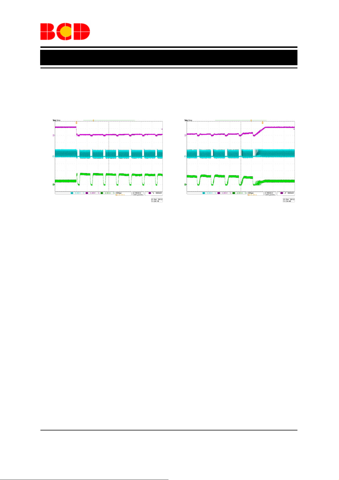
Figure 12. Short Circuit Protection (I
I
L
2A/di
Time (400μs/div)
=1A) Figure 13. Short Circuit Protection Recovery (I
OUT
OUT
=1A)
Mar. 2013 Rev. 1.0 BCD Semiconductor Manufacturing Limited
8
Page 9
Preliminary Datasheet
Dual 1A, 1.5MHZ Synchronous Step-down DC-DC Converter AP3427M
Typical Application
C
OUT1
10 µF
V
OUT1
L1 2.2µH
Connected
to V
IN
C
IN2
4.7µF
C1
option
R2
R1
110
2
FB1
3
VIN2
GND
56
LX2 EN2
AP3427M
LX1EN1
GND
VIN1
FB2
9
8
74
R3
R4
C2
option
C
IN1
4.7µF
VIN= 2.5V to 5.5V
Note 2: V
OUT1=VFB1
×(1+R1/R2) ; V
L2 2.2µH
=V
OUT2
Figure 14. Typical Application of AP3427M (Note 2)
×(1+R3/R4), and R2=R4=10kΩ is recommended.
FB2
C
OUT2
10µF
V
OUT2
Mar. 2013 Rev. 1.0 BCD Semiconductor Manufacturing Limited
9
Page 10
Preliminary Datasheet
Dual 1A, 1.5MHZ Synchronous Step-down DC-DC Converter AP3427M
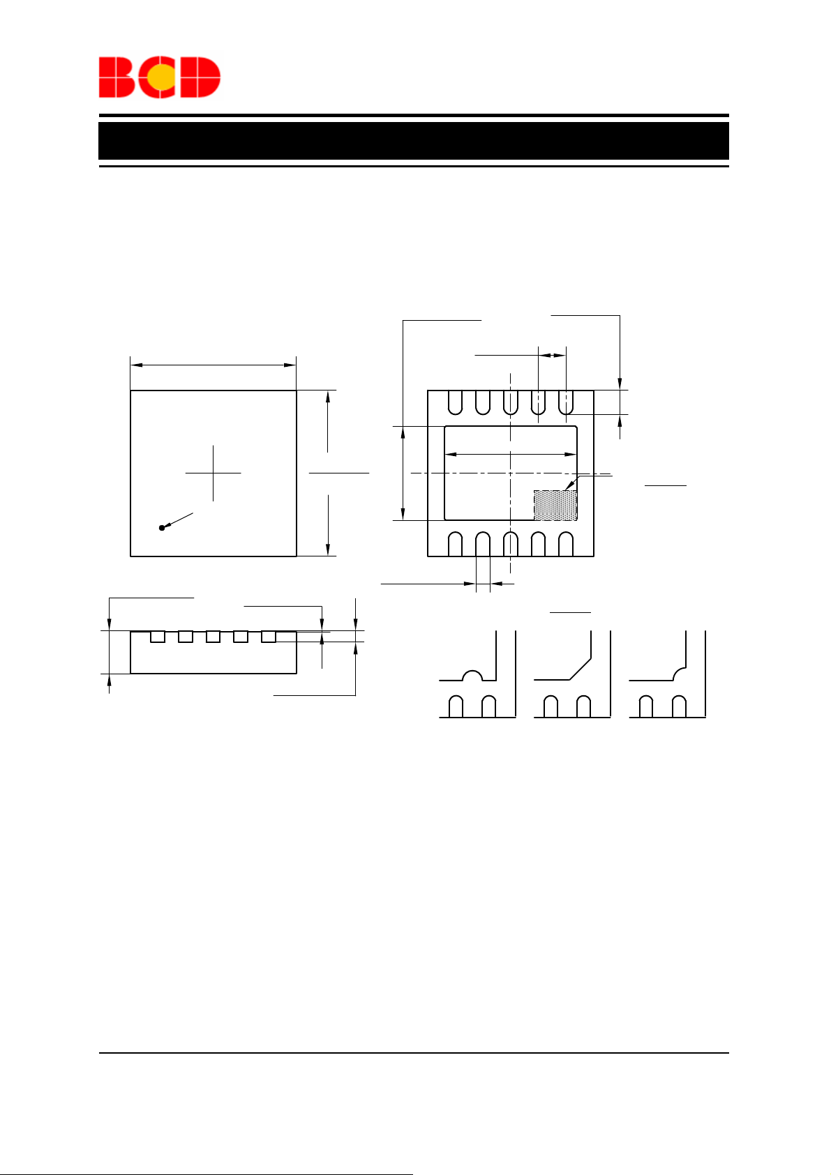
Mechanical Dimensions
DFN-3×3-10 Unit: mm(inch)
0.700(0.028)
0.800(0.031)
2.900(0.114)
3.100(0.122)
Pin 1 Mark
0.000(0.000)
0.050(0.002)
2.900(0.114)
3.100(0.122)
1.600(0.063)
1.800(0.071)
0.200(0.008)
0.300(0.012)
0.500(0.020)
TYP
N6 N10
2.300(0.090)
2.500(0.098)
N5
0.300(0.012)
0.500(0.020)
PIN #1 IDENTIFICATION
See DETAIL A
N1
DETAIL A
0.153(0.006)
0.253(0.010)
12
12
Pin 1 options
12
Mar. 2013 Rev. 1.0 BCD Semiconductor Manufacturing Limited
10
Page 11

BCD Semiconductor Manufacturing Limited
IMPORTANT NOTICE
http://www.bcdsemi.com
BCD Semiconductor Manufacturing Limited reserves the right to make changes without further notice to any products or specifications herein. BCD Semiconductor Manufacturing Limited does not assume any responsibility for use of any its products for any
IMPORTANT NOTICE
IMPORTANT NOTICE
particular purpose, nor does BCD Semiconductor Manufacturing Limited assume any liability arising out of the application or use
of any its products or circuits. BCD Semiconductor Manufacturing Limited does not convey any license under its patent rights or
BCD Semiconductor Manufacturing Limited reserves the right to make changes without further notice to any products or specifi-
BCD Semiconductor Manufacturing Limited reserves the right to make changes without further notice to any products or specifi-
other rights nor the rights of others.
cations herein. BCD Semiconductor Manufacturing Limited does not assume any responsibility for use of any its products for any
cations herein. BCD Semiconductor Manufacturing Limited does not assume any responsibility for use of any its products for any
particular purpose, nor does BCD Semiconductor Manufacturing Limited assume any liability arising out of the application or use
particular purpose, nor does BCD Semiconductor Manufacturing Limited assume any liability arising out of the application or use
MAIN SITE
of any its products or circuits. BCD Semiconductor Manufacturing Limited does not convey any license under its patent rights or
of any its products or circuits. BCD Semiconductor Manufacturing Limited does not convey any license under its patent rights or
- Headquarters
BCD (Shanghai) Micro-electronics Limited
other rights nor the rights of others.
other rights nor the rights of others.
No. 1600, Zi Xing Road, Shanghai ZiZhu Science-based Industrial Park, 200241, P. R.C.
Tel: +86-021-2416-2266, Fax: +86-021-2416-2277
MAIN SITE
MAIN SITE
REGIONAL SALES OFFICE
- Headquarters
BCD Semiconductor Manufacturing Limited
BCD Semiconductor Manufactur ing Limited
Shenzhen Office
- Wafer Fab
No. 1600, Zi Xing Road, Shanghai ZiZhu Science-based Industrial Park, 200241, China
Shanghai SIM-BCD Semiconductor Manufacturing Co., Ltd., Shenzhen Office
Shanghai SIM-BCD Semiconductor Manufacturing Limited
Tel: +86-21-24162266, Fax: +86-21-24162277
Unit A Room 1203,Skyworth Bldg., Gaoxin Ave.1.S., Nanshan District
800, Yi Shan Road, Shanghai 200233, China
Shenzhen 518057, China
Tel: +86-21-6485 1491, Fax: +86-21-5450 0008
REGIONAL SALES OFFICE
Tel: +86-0755-8660-4900, Fax: +86-0755-8660-4958
Shenzhen Office
REGIONAL SALES OFFICE
Shanghai SIM-BCD Semiconductor Manufacturing Co., Ltd., Shenzhen Office
Taiwan Office (Hsinchu)
Shenzhen Office
Unit A Room 1203, Skyworth Bldg., Gaoxin Ave.1.S., Nanshan District, Shenzhen,
BCD Semiconductor (Taiwan) Company Limited
Shanghai SIM-BCD Semiconductor Manufacturing Co., Ltd. Shenzhen Office
China
8F, No.176, Sec. 2, Gong-Dao 5th Road, East District
Advanced Analog Circuits (Shanghai) Corporation Shenzhen Office
Tel: +86-755-8826 7951
HsinChu City 300, Taiwan, R.O.C
Room E, 5F, Noble Center, No.1006, 3rd Fuzhong Road, Futian District, Shenzhen 518026, China
Fax: +86-755-8826 7865
Tel: +886-3-5160181, Fax: +886-3-5160181
Tel: +86-755-8826 7951
Fax: +86-755-8826 7865
- Wafer Fab
Shanghai SIM-BCD Semiconductor Manufacturing Co., Ltd.
800 Yishan Road, Shanghai 200233, China
Tel: +021-6485-1491, Fax: +86-021-5450-0008
- Wafer Fab
BCD Semiconductor Manufacturing Limited
Shanghai SIM-BCD Semiconductor Manufacturing Co., Ltd.
Taiwan Office (Taipei)
- IC Design Group
800 Yi Shan Road, Shanghai 200233, China
BCD Semiconductor (Taiwan) Company Limited
Advanced Analog Circuits (Shanghai) Corporation
Tel: +86-21-6485 1491, Fax: +86-21-5450 0008
3F, No.17, Lane 171, Sec. 2, Jiu-Zong Rd., Nei-Hu Dist., Taipei(114), Taiwan, R.O.C
8F, Zone B, 900, Yi Shan Road, Shanghai 200233, China
Tel: +886-2-2656 2808
Tel: +86-21-6495 9539, Fax: +86-21-6485 9673
Fax: +886-2-2656-2806/26562950
Taiwan Office
BCD Semiconductor (Taiwan) Company Limited
USA Office
Taiwan Office
4F, 298-1, Rui Guang Road, Nei-Hu District, Taipei,
BCD Semiconductor Corp.
BCD Semiconductor (Taiwan) Company Limited
Tai wan
48460 Kato Road, Fremont, CA 94538, USA
4F, 298-1, Rui Guang Road, Nei-Hu District, Taipei,
Tel: +886-2-2656 2808
Tel: +1-510-668-1950
Taiwan
Fax: +886-2-2656 2806
Fax: +1-510-668-1990
Tel: +886-2-2656 2808
Fax: +886-2-2656 2806
USA Office
Korea Office
BCD Semiconductor Limited Korea office.
Room 101-1112, Digital-Empire II, 486 Sin-dong,
Yeongtong-Gu, Suwon-city, Gyeonggi-do, Korea
Tel: +82-31-695-8430
BCD Semiconductor Corp.
USA Office
30920 Huntwood Ave. Hayward,
BCD Semiconductor Corporation
CA 94544, USA
30920 Huntwood Ave. Hayward,
Tel : +1-510-324-2988
CA 94544, U.S.A
Fax: +1-510-324-2788
Tel : +1-510-324-2988
Fax: +1-510-324-2788
 Loading...