

Page 1

1.3MHz, Dual 1.0A Synchronous Step-down Converters AP3421/A/B
Preliminary Datasheet
General Description
The AP3421/A/B is a fully integrated dual output
voltage regulator. The two converters are current
mode and internally compensated. The converters
include integrated control and synchronous rectifier
switches. The outputs are both rated for up to 1A.
Both outputs are adjustable using external resistors.
The step-down converters operate at 1.3MHz fixed
switching frequency under normal load and in a pulse
skipping mode for light loads. The switching clock is
shifted 180° for SW2. The E/S pin provides an enable
function and allows the converter to be synchronized
to an external clock. With E/S held low, the
AP3421/A/B draws less than 10µA current.
In the start-up sequence, the VO1 output is designed
to precede the VO2 output. The two outputs have
controlled start-up sequence.
Power On Reset (POR) function is provided by
means of an open-drain output present on the POR
pin. The POR function monitors VMON, FB1 and
FB2, and pulls low if any of these begin to drop out.
The POR is internally deglitched and provides a
delayed recovery/reset time.
The AP3421/A/B provides peak over-current
protection, short circuit protection and thermal
shutdown. Discharge-Before-Turn-On discharges the
outputs completely before soft-starting to always
bring them up in the proper sequence at start-up or
after a POR (For AP3421/A only).
The AP3421/A/B is available in DFN-3×3-10
package.
Features
• V
• V
• Switching Frequency: 1.3MHz
• 180° Phase Shifted Switching
• No Rectifier Diode Required
• Optional Exter nal Cl ocking (2× Clock Required)
• Light Load Pulse Skipping
• Enable/Sleep State
• Internal Soft-start
• Open-drain Power On Reset Monitors Input and
• Outputs
• Discharge-Before-Turn-On (For AP3421/A)
• Pre-bias Function (For AP3421B)
• Peak Over Current Protection
• Short Circuit Protection
• Over Temperature Shutdown
=1.8 to 3.6V at 1A
O1
=1.0 to 3.6V at 1A
O2
Applications
• Hard Disk Drivers
• Set Top Boxes
DFN-3×3-10
Figure 1. Package Type of AP3421/A/B
Feb. 2013 Rev. 1. 4 BCD Semiconductor Manufacturing Limited
1
Page 2
µ
Preliminary Datasheet
1.3MHz, Dual 1.0A Synchronous Step-down Converters AP3421/A/B
Pin Configuration
DN Package
(DFN-3×3-10)
Pin 1 Mark
1
2
3
4
56
10
9
8
7
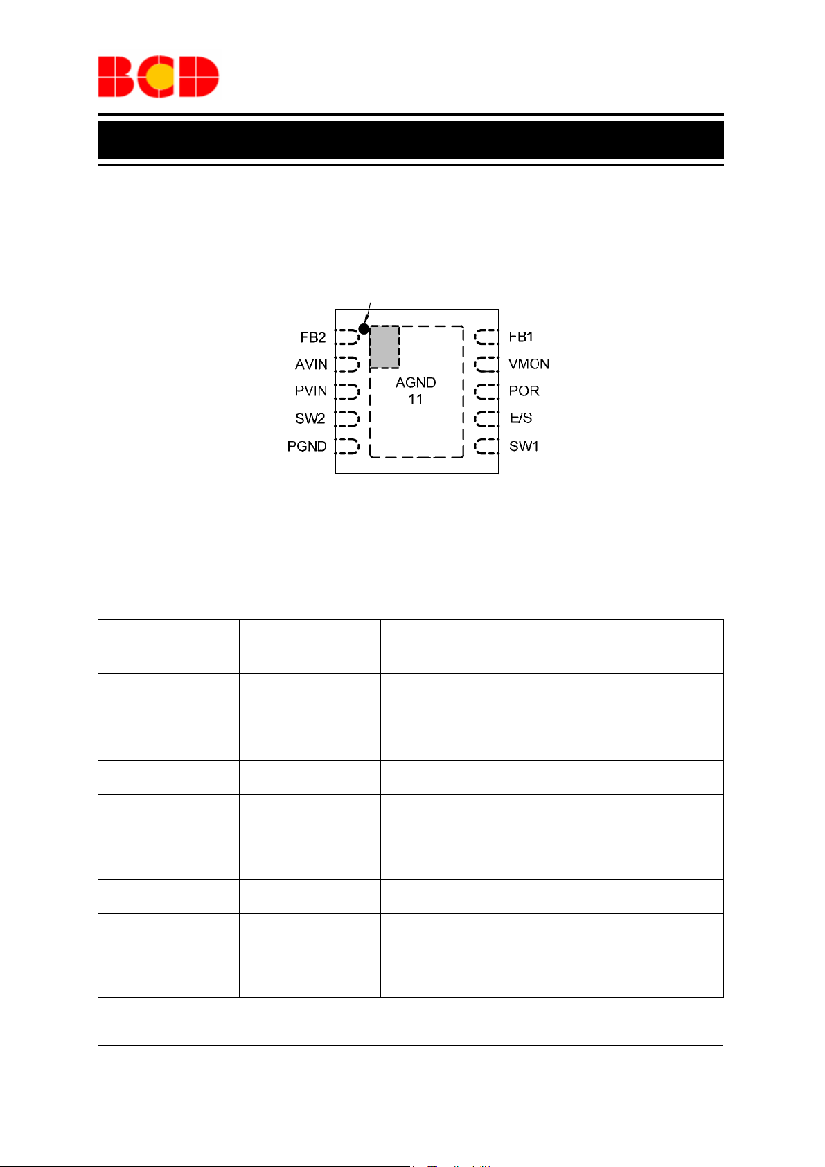
Figure 2. Pin Configuration of AP3421/A/B (Top View)
Pin Description
Pin Number Pin Name Function
1 FB2
2 AVIN
3 PVIN
4 SW2
5 PGND
6 SW1
7 E/S
Feedback from VO2. Connect voltage divider to the
load side of VO2 output inductor-capacitor filter
Analog power input. Connect a 1µF ceramic capacitor
between this pin and AGND
Control MOSFET switch power input. Connect a 10
ceramic capacitor between this pin and PGND, as close
to the IC as possible
VO2 synchronous buck switching output. Connect to
VO2 inductor
Power ground connection. Synchronous rectifier
MOSFET source. Provide a star connection between
this pin, VO1, VO2 filter capacitor returns, VIN input
capacitor return, and AGND. Keep the star connection
as close to the IC as possible
VO1 synchronous buck switching output. Connect to
VO1 inductor
Enable/Synchronization. Pulling this pin high statically
enables the IC and pulling the pin low statically will
shut down the IC. Applying a pulse to this pin will
synchronize SW1 and SW2 switching frequency to ½
the external clock frequency
F
Feb. 2013 Rev. 1. 4 BCD Semiconductor Manufacturing Limited
2
Page 3

Preliminary Datasheet
1.3MHz, Dual 1.0A Synchronous Step-down Converters AP3421/A/B
Pin Description (Continued)
Pin Number Pin Name Function
Power on reset output pin. Monitors FB1, FB2 output
8 POR
9 VMON
10 FB1
11 AGND
voltage levels and V
voltage drop is detected on FB1 or FB2 or VIN, and is
Hi-Z during normal operation
Voltage monitor–supervisor for one external voltage
(could be input voltage). The POR output is triggered if
this output falls below the VMON threshold
Feedback from VO1. Connect voltage divider to the
load side of VO1 output inductor-capacitor filter
Signal ground connection. Provide a star connection
between this pin and PGND pin
. POR is pulled low if an output
IN
Feb. 2013 Rev. 1. 4 BCD Semiconductor Manufacturing Limited
3
Page 4
Preliminary Datasheet
1.3MHz, Dual 1.0A Synchronous Step-down Converters AP3421/A/B
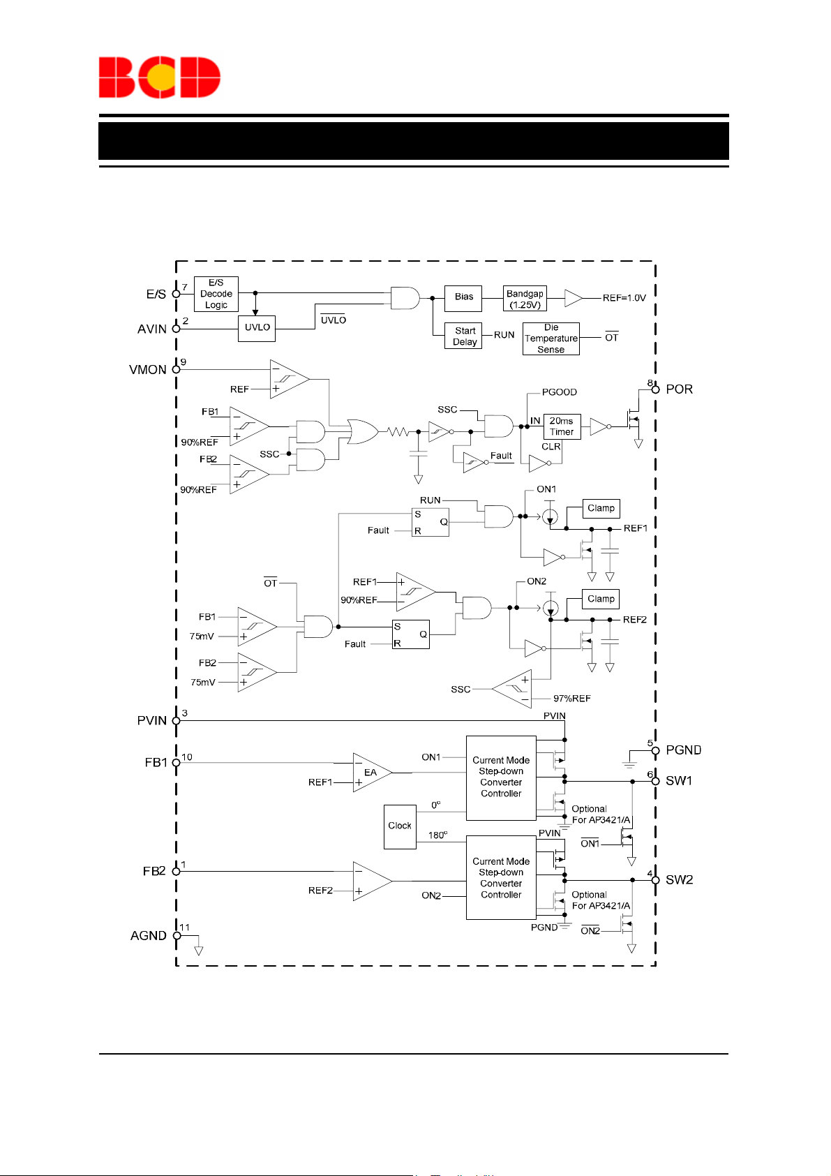
Functional Block Diagram
Figure 3. Functional Block Diagram of AP3421/A/B
Feb. 2013 Rev. 1. 4 BCD Semiconductor Manufacturing Limited
4
Page 5
θ
Preliminary Datasheet
1.3MHz, Dual 1.0A Synchronous Step-down Converters AP3421/A/B
Ordering Information
AP3421 -
Circuit Type
A: AP3421A
B: AP3421B
Blank: AP3421
Package
DN: DFN-3×3-10
G1: Green
TR: Tape & Reel
Package
DFN-3×3-10 -40 to 85°C
Temperature
Range
Part Number Marking ID Packing Type
AP3421DNTR-G1 BCB
Tape & Reel AP3421ADNTR-G1 BDD
AP3421BDNTR-G1 BDE
BCD Semiconductor's Pb-free products, as designated with "G1" suffix in the part number, are RoHS compliant
and green.
Absolute Maximum Ratings (Note 1)
Parameter Symbol Value Unit
Input Voltage VIN -0.3 to 7 V
Feedback Voltage VFB -0.3 to VIN+0.3 V
E/S Pin Voltage V
SW1, SW2 Pin Voltage VSW V
Thermal Resistance
-0.3 to VIN+0.3 V
E/S
-1 to VIN+1 V
PGND
JA
33 ºC /W
Operating Junction Temperature TJ 150 ºC
Storage Temperature T
Lead Temperature (Soldering, 10sec) T
Note 1: Stresses greater than those listed under “Absolute Maximum Ratings” may cause permanent damage to
the device. These are stress ratings only, and functional operation of the device at these or any other conditions
beyond those indicated under “Recommended Operating Conditions” is not implied. Exposure to “Absolute
Maximum Ratings” for extended periods may affect device reliability.
-25 to 150 ºC
STG
260 ºC
LEAD
Recommended Operating Conditions
Parameter Symbol Min Max Unit
Input Voltage V
IN
VO1 Maximum Output Current IO1(Max) 1 A
VO2 Maximum Output Current IO2(Max) 1 A
Operating Ambient Temperature TA -40 85
Feb. 2013 Rev. 1. 4 BCD Semiconductor Manufacturing Limited
AP3421 4.5 5.5
AP3421A/B 3.0 5.5
V
°C
5
Page 6

µ
Preliminary Datasheet
1.3MHz, Dual 1.0A Synchronous Step-down Converters AP3421/A/B
Electrical Characteristics
V
IN =VE/S
Parameter Symbol Conditions Min Typ Max Unit
Operating Input Voltage VIN
Supply Current ICC V
Shutdown Supply Current I
Under Voltage Lockout Threshold
Under Voltage Lockout Hysteresis V
POR Threshold VMON V
Feedback Voltage V
Switch Current Limit
Oscillator Frequency f
Soft-start Time t
POR Threshold FB1 V
POR Threshold FB2 V
Discharge Complete Threshold
(AP3421/A )
E/S Pin Threshold
Frequency Lock-in Range
POR Assert Delay Time t
POR Release Delay Time t
POR Low Voltage V
VO2 Start Threshold (AP3421/A ) V
SW1, SW2 Discharge Resistance R
Internal
MOSFET on
Resistance
Thermal Shutdown Threshold T
Thermal Shutdown Hysteresis T
=5V, TA=25℃, unless otherwise specified.
AP3421,
AP3421A/B
AP3421A/B
AP3421 4.5 5.0 5.5
AP3421A/B 3.0 3.3 5.5
FB1=VFB2
V
SHDN
AP3421
AP3421A/B 2.4 2.7 3.0
HUVLO
VMON_POR
FB1, VFB2
OSC1
V
I
1.2 1.6
LIM1
I
1.2 1.6
LIM2
, f
1.0 1.30 1.60 MHz
OSC2
0.5 1.0 2.0 ms
SS_FB1
FB11Falling1 86 89 92 %V
FB1_POR
FB21Falling1 86 89 92 %V
FB2_POR
E/S
Rising Edge
300 mV
VMON
0.975 1.0 1.025 V
=1.2V 1.0 mA
=0V, VIN=5.0V 10
3.0 3.5 4.0
Falling 0.97 1.00 1.03 V
FB1 Level Where
V
FB1_DCT
Discharge Cycle Is
50 75 100 mV
Terminated
V
EN_L
V
1.5
EN_H
f
E/S_MIN
f
SWITCHING
=50%×f
E/S
0.6 V
1.5
When Externally
f
3.0
E/S_MAX
POR_DELAY
POR_HOLD
POR_LOW
Clocked
Fault Flag Set to
POR Pull Low
Fault Flag Reset to
POR Hi-Z State
10 25 40
10 20 30 ms
POR Sinking 4mA 300 mV
FB1 Rising Voltage
FB1_ST
for FB2 to Initiate
86 89 92 %V
Soft-start
Discharge1Resistan-
STOP_SW1,2
R
DS_SW1_U
R
DS_SW2_U
R
DS_SW1_L
R
DS_SW2_L
R
DS_SW1_U
R
DS_SW2_U
R
DS_SW1_L
R
DS_SW2_L
ce for SW1, SW2
V
=5.0V
IN
ISW=100mA
260
160
280
180
160 ºC
OTSD
10 20 30 ºC
HYS
=5.0V
V
IN
ISW=-100mA
=3.3V
V
IN
ISW=100mA
=3.3V
V
IN
=-100mA
I
SW
15 30 45
277
249
300
260
MHz
V
A
V
A
FB1
FB2
µs
FB1
Ω
mΩ
Feb. 2013 Rev. 1. 4 BCD Semiconductor Manufacturing Limited
6
Page 7

Preliminary Datasheet
1.3MHz, Dual 1.0A Synchronous Step-down Converters AP3421/A/B
Typical Performance Characteristics
VIN=V
=5V, VO1=2.5V, VO2=1.2V, L1=L2=3.3µH, C1=C3=10µF, C2=C2’=10µF, TA=25°C, unless
E/S
otherwise specified.
1200
1000
800
600
400
SW1, SW2 Frequency (kHz)
200
3.43.63.84.04.24.44.64.85.05.25.45.65.8
Input Voltage (V)
0.66
0.64
0.62
0.60
0.58
0.56
0.54
Supply Current (mA)
0.52
0.50
0.48
-60 -40 -20 0 20 40 60 80 100 120 140
Figure 4. SW1, SW2 Frequency vs. Input Voltage Figure 5. Supply Current vs. Temperature
2.0
1.8
2.0
1.8
1.6
1.4
1.2
1.0
Current Limit 1 (A)
0.8
1.6
1.4
1.2
1.0
Current Limit 2 (A)
0.8
0.6
-60 -40 -20 0 20 40 60 80 100 120 140
Temperature (OC)
0.6
-60 -40 -20 0 20 40 60 80 100 120 140
Figure 6. Current Limit 1 vs. Temperature
Figure 7. Current Limit 2 vs. Temperature
Temperature (oC)
Temperature (OC)
V
FB1=VFB2
=1.2V
Feb. 2013 Rev. 1. 4 BCD Semiconductor Manufacturing Limited
7
Page 8

Preliminary Datasheet
1.3MHz, Dual 1.0A Synchronous Step-down Converters AP3421/A/B
Typical Performance Characteristics (Continued)
VIN=V
=5V, VO1=2.5V, VO2=1.2V, L1=L2=3.3µH, C1=C3=10µF, C2=C2’=10µF, TA=25°C, unless
E/S
otherwise specified.
2.60
2.58
2.56
2.54
2.52
2.50
2.48
2.46
VO1 Voltage (V)
2.44
2.42
2.40
200 400 600 800 1000 1200
Output Current (mA)
VO2=1.2V, IO2=1A
1.300
1.275
1.250
1.225
1.200
1.175
VO2 Voltage (V)
1.150
1.125
1.100
1.075
1.050
1.025
1.000
200 400 600 800 1000 1200 1400
VO1=2.5V, IO1=1A
Output Current (mA)
Figure 8. VO1 Voltage vs. Output Current Figure 9. VO2 Voltage vs. Output Current
100
95
90
85
80
75
70
65
60
VO1 Efficiency (%)
55
50
45
40
200 400 600 800 1000 1200
Output Current (mA)
VO1=2.5V
100
95
90
85
80
75
70
65
60
55
50
45
VO2 Efficiency (%)
40
35
30
25
20
200 400 600 800 1000 1200 1400
VO2=1.2V
Output Current (mA)
Figure 10. VO1 Efficiency vs. Output Current Figure 11. VO2 Efficiency vs. Output Current
Feb. 2013 Rev. 1. 4 BCD Semiconductor Manufacturing Limited
8
Page 9

Preliminary Datasheet
1.3MHz, Dual 1.0A Synchronous Step-down Converters AP3421/A/B
Typical Performance Characteristics (Continued)
VIN=V
=5V, VO1=2.5V, VO2=1.2V, L1=L2=3.3µH, C1=C3=10µF, C2=C2’=10µF, TA=25°C, unless
E/S
otherwise specified.
V
IN
2V/div
V
O1
2V/div
V
O2
1V/div
V
POR
2V/div
V
2V/div
V
1V/div
V
5V/div
V
POR
5V/div
01
O2
IN
Time 4ms/div Time 400µs/div
Figure 12. Start-up from VIN Figure 13. Power-down from VIN
I
O1
500mA/div
(AC)
V
O1
100mV/div
I
O2
500mA/div
(AC)
V
O2
50mV/div
Time 100µs/div Time 100µs/div
Figure 14. Load Transient Figure 15. Load Transient
(VO=2.5V IO=0.5A to 1.0A) (VO=1.2V IO=0.5A to 1.0A)
Feb. 2013 Rev. 1. 4 BCD Semiconductor Manufacturing Limited
9
Page 10

Preliminary Datasheet
1.3MHz, Dual 1.0A Synchronous Step-down Converters AP3421/A/B
Typical Performance Characteristics (Continued)
VIN=V
=5V, VO1=2.5V, VO2=1.2V, L1=L2=3.3µH, C1=C3=10µF, C2=C2’=10µF, TA=25°C, unless
E/S
otherwise specified.
Output 1
Induction
Current
1A/div
V
5V/div
Output 2
Induction
Current
20mA/div
IN
Output 1
Induction
Current
1A/div
V
5V/div
Output 2
Induction
Current
1A/div
IN
Time 40µs/div Time 40µs/div
Figure 16. Short Protection for Output 1 Figure 17. Short Protection for Output 2
V
2V/div
V
2V/div
V
2V/div
Output 1
Induction
Current
1A/div
IN
O1
O2
Output 2
Induction
Current
1A/div
V
2V/div
V
2V/div
V
2V/div
IN
O1
O2
Time 10ms/div Time 10ms/div
Figure 18. Output 1 Short Recovery Figure 19. Output 2 Short Recovery
Feb. 2013 Rev. 1. 4 BCD Semiconductor Manufacturing Limited
10
Page 11

Preliminary Datasheet
1.3MHz, Dual 1.0A Synchronous Step-down Converters AP3421/A/B
Application Information
1. Operation
The DC-DC converters are current-mode buck
converters with a synchronous rectifier and internal
compensation. They are designed to be stable with a
1.5µH to 6.8µH inductor value and 10µF to 22µF
output capacitor. Both output voltages are resistor
programmable. The switching frequency of the
converter is fixed and the switches turn on at
alternating 180° phase intervals.
The converter operates in 2 possible modes:
Continuous Mode (CM), and Pulse Skipping Mode
(PSM). CM is the default mode under normal loading.
Under light loads, PSM mode occurs, where
switching cycles are skipped if the current demand is
low.
2. Soft-start
The DC-DC converter contains a soft-start function
that brings the output voltages up in a slowly
increasing ramp with any resistive load from open
circuit to 1A (resistive) and any capacitor from 10µF
to 22µF. During soft-start, the peak inductor current
shall not exceed 750mA until the output voltage
reaches 25% of its final value. Current limit shall be
active but not trip during soft-start into a rated
resistive load. Overshoot voltage during soft-start is
limited to 1%.
3. Power Sequencing and Enable
When power is applied and if E/S input is asserted
(High) or is toggling, the DC-DC converters will
enter RUN mode after a short settling period. If the
E/S pin is a static low, the IC will enter a SLEEP
state where it draws very little input current.
When in RUN mode, if there is no fault condition, the
VO1 output (SW1) will be the first output to begin
soft-start. When the reference voltage for FB1
reaches approximately 90% of the final value, the
VO2 output (SW2) will begin soft-start.
4. POR
Under voltage comparators are provided to monitor
the output voltages and VMON which could be the
input voltage. If any of these voltages falls below its
POR threshold, a POR open drain output will turn on
which pulls the POR pin low. After the POR
condition is cleared, there is a delay of 20ms before
Feb. 2013 Rev. 1. 4 BCD Semiconductor Manufacturing Limited
th
the POR output transistor is turned off; when off the
POR pin is high-Z and may be pulled up high with a
resistor. The POR function has built-in deglitching.
Once the POR is detected, the power supply outputs
will be discharged prior to restart using the
soft-start/sequencing routine.
5.1Over Current and Short Circuit
Protection
The DC-DC converters shall have over current and
short circuit protection. Under any load condition , at
any time, any value of load resistor (including 0Ω)
can be applied to the DC-DC outputs instantaneously
and held in place indefinitely without the switch
current exceeding the peak current limit and withou t
the IC suffering any permanent damage or loss of
performance. The output voltage is allowed to drop
under over current or short circuit conditions.
Recovery to output voltage regulation is required
within 10ms of the instant the loading is reduced to
maximum allowable rated load; the output voltage
shall not exceed the dynamic load excursion limits
(±5% excursion) upon recovery. Over current shall
not be triggered by a sudden rate of load current
change provided the loading does not exceed the
output load rating of 1A.
6. E/S Function
Enable/Synchronization function. Pulling this pin
high statically enables the AP3421/A/B while pulling
the pin low statically for longer than 4µs will shut
down the AP3421/A/B. Applying a pulse to this pin
will synchronize SW1 and SW2 switching frequency
to ½ the external clock frequency. The external
frequency lock-in ranges from 1.5MHz to 3.0MHz.
11
Page 12

Preliminary Datasheet
1.3MHz, Dual 1.0A Synchronous Step-down Converters AP3421/A/B
Typical Application
VIN=5V
C1'
1
POR
SW2
FB2
F
84.5k
24.9k
L2 3.3
4.7k
C2
10
=1.2VVO1=2.5V
V
O2
C2'
F
10
F
4.02k
20k
OFF ON
30.1k
20k
C3
10
C1
10
F
F
PVIN AVIN VMON
E/S
L1 3.3
SW1
AGND
FB1
PGND
Figure 20. Typical Application Circuit of AP3421 (Note 2)
Feb. 2013 Rev. 1. 4 BCD Semiconductor Manufacturing Limited
12
Page 13

Preliminary Datasheet
1.3MHz, Dual 1.0A Synchronous Step-down Converters AP3421/A/B
Typical Application (Continued)
VIN=3.3 to 5V
C1'
1
POR
SW2
FB2
F
36k
18k
L2 3.3
4.7k
C2
10
=1.2VVO1=2.5V
V
O2
C2'
F
10
F
4.02k
20k
OFF ON
30.1k
20k
C3
10
C1
10
F
F
PVIN AVIN VMON
E/S
L1 3.3
SW1
FB1
AGND
PGND
Figure 21. Typical Application Circuit of AP3421A /B (Note 2)
Note 2: AVIN and PVIN pin should not be connected together directly to avoid disturbance between them in
PCB layout:
1) Place a 1.0µF capacitor between AVIN pin and AGND for power filtering.
2) Place a 10µF capacitor between PVIN pin and PGND for power filtering.
Feb. 2013 Rev. 1. 4 BCD Semiconductor Manufacturing Limited
13
Page 14

Preliminary Datasheet
1.3MHz, Dual 1.0A Synchronous Step-down Converters AP3421/A/B
Mechanical Dimensions
DFN-3×3-10 Unit: mm(inch)
Feb. 2013 Rev. 1. 4 BCD Semiconductor Manufacturing Limited
14
Page 15

BCD Semiconductor Manufacturing Limited
IMPORTANT NOTICE
IMPORTANT NOTICE
BCD Semiconductor Manufacturing Limited reserves the right to make changes without further notice to any products or specifi-
BCD Semiconductor Manufacturing Limited reserves the right to make changes without further notice to any products or specifi-
cations herein. BCD Semiconductor Manufacturing Limited does not assume any responsibility for use of any its products for any
cations herein. BCD Semiconductor Manufacturing Limited does not assume any responsibility for use of any its products for any
particular purpose, nor does BCD Semiconductor Manufacturing Limited assume any liability arising out of the application or use
particular purpose, nor does BCD Semiconductor Manufacturing Limited assume any liability arising out of the application or use
of any its products or circuits. BCD Semiconductor Manufacturing Limited does not convey any license under its patent rights or
of any its products or circuits. BCD Semiconductor Manufacturing Limited does not convey any license under its patent rights or
other rights nor the rights of others.
other rights nor the rights of others.
http://www.bcdsemi.com
MAIN SITE
MAIN SITE
- Headquarters
BCD Semiconductor Manufacturing Limited
BCD Semiconductor Manufactur ing Limited
- Wafer Fab
No. 1600, Zi Xing Road, Shanghai ZiZhu Science-based Industrial Park, 200241, China
Shanghai SIM-BCD Semiconductor Manufacturing Limited
Tel: +86-21-24162266, Fax: +86-21-24162277
800, Yi Shan Road, Shanghai 200233, China
Tel: +86-21-6485 1491, Fax: +86-21-5450 0008
REGIONAL SALES OFFICE
Shenzhen Office
REGIONAL SALES OFFICE
Shanghai SIM-BCD Semiconductor Manufacturing Co., Ltd., Shenzhen Office
Shenzhen Office
Unit A Room 1203, Skyworth Bldg., Gaoxin Ave.1.S., Nanshan District, Shenzhen,
Shanghai SIM-BCD Semiconductor Manufacturing Co., Ltd. Shenzhen Office
China
Advanced Analog Circuits (Shanghai) Corporation Shenzhen Office
Tel: +86-755-8826 7951
Room E, 5F, Noble Center, No.1006, 3rd Fuzhong Road, Futian District, Shenzhen 518026, China
Fax: +86-755-8826 7865
Tel: +86-755-8826 7951
Fax: +86-755-8826 7865
- Wafer Fab
BCD Semiconductor Manufacturing Limited
Shanghai SIM-BCD Semiconductor Manufacturing Co., Ltd.
- IC Design Group
800 Yi Shan Road, Shanghai 200233, China
Advanced Analog Circuits (Shanghai) Corporation
Tel: +86-21-6485 1491, Fax: +86-21-5450 0008
8F, Zone B, 900, Yi Shan Road, Shanghai 200233, China
Tel: +86-21-6495 9539, Fax: +86-21-6485 9673
Taiwan Office
BCD Semiconductor (Taiwan) Company Limited
Taiwan Office
4F, 298-1, Rui Guang Road, Nei-Hu District, Taipei,
BCD Semiconductor (Taiwan) Company Limited
Tai wan
4F, 298-1, Rui Guang Road, Nei-Hu District, Taipei,
Tel: +886-2-2656 2808
Taiwan
Fax: +886-2-2656 2806
Tel: +886-2-2656 2808
Fax: +886-2-2656 2806
USA Office
BCD Semiconductor Corp.
USA Office
30920 Huntwood Ave. Hayward,
BCD Semiconductor Corporation
CA 94544, USA
30920 Huntwood Ave. Hayward,
Tel : +1-510-324-2988
CA 94544, U.S.A
Fax: +1-510-324-2788
Tel : +1-510-324-2988
Fax: +1-510-324-2788
 Loading...