

Page 1
1.2A, 1.4MHz High Efficiency Synchronous DC-DC Buck Converter AP3407/A
Data Sheet
General Description
The AP3407/A is a 1.4MHz fixed frequency, current
mode, PWM synchronous buck (step-down) DC-DC
converter, capable of driving a 1.2A load with high
efficiency, excellent line and load regulation. The
device integrates synchronous P-channel and
N-channel power MOSFET switches with low
on-resistance. It is ideal for powering portable
equipment that runs from a single Li-ion battery.
A standard series of inductors are available from
several different manufacturers optimized for use
with the AP3407/A. This feature greatly simplifies
the design of switch-mode power supplies.
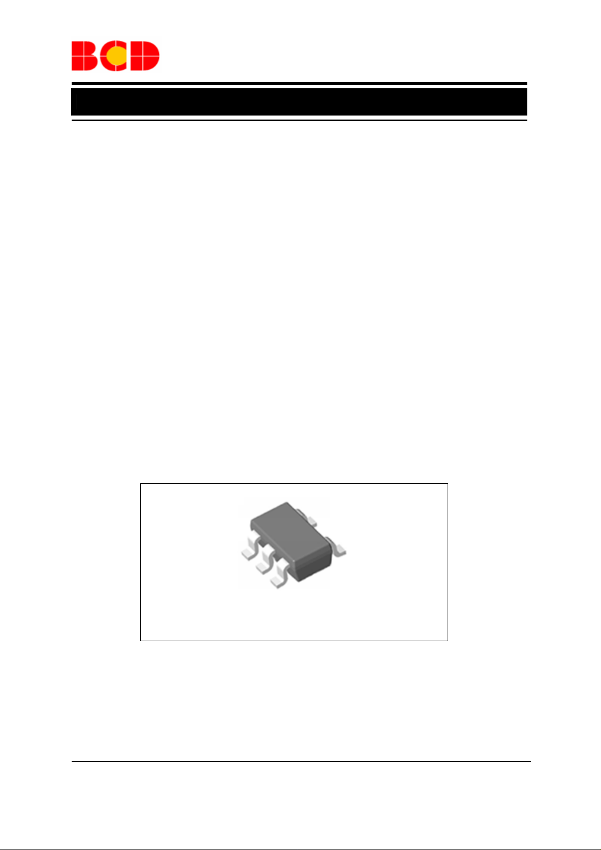
The AP3407/A is available in SOT-23-5.
Features
Input Voltage Range: 2.5V to 5.5V
•
• Output Voltage: 0.6V to V
• ADJ Output
• Fixed 1.4MHz Frequency
• High Efficiency up to 95%
• Output Current: 1.2A
• Current Mode Control
• 100% Duty Cycle in Dropout
• Built-in Over Current Protection
• Built-in Short Circuit Protection
• Built-in Thermal Shutdown Protection
• Built-in UVLO Function
• Built-in Soft-start
IN
Applications
• Datacom
• Portable Device
• Smart Phone
SOT-23-5
Figure 1. Package Type of AP3407/A
Dec. 2011 Rev. 1. 3 BCD Semiconductor Manufacturing Limited
1
Page 2
Data Sheet
1.2A, 1.4MHz High Efficiency Synchronous DC-DC Buck Converter AP3407/A
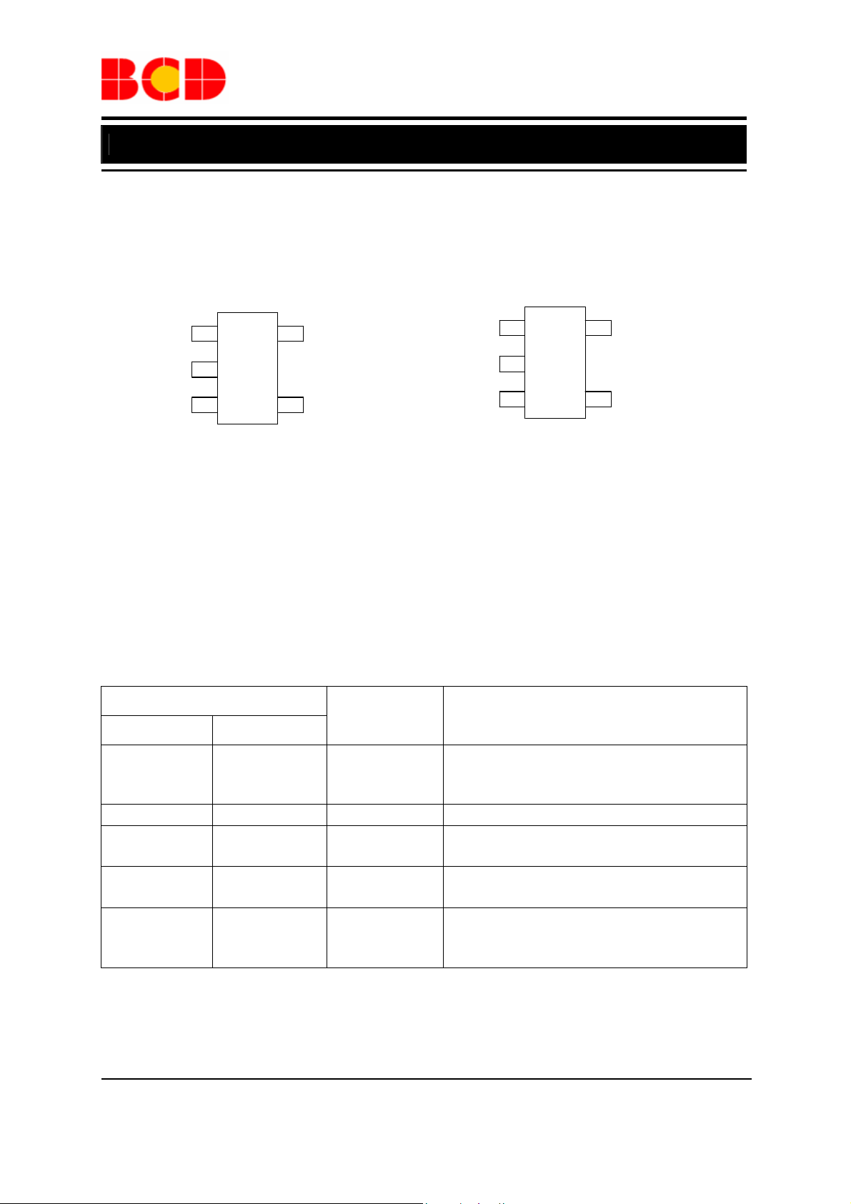
Pin Configuration
K Package
(SOT-23-5)
1
EN
GND
2
SW
34
(For AP3407) (For AP3407A)
Pin Description
Pin Number
AP3407 AP3407A
1 3 EN
2 2 GND Ground pin
3 5 SW
5
FB
VIN
1
VIN
GND
2
EN
34
Figure 2. Pin Configuration of AP3407/A (Top View)
Pin Name Function
Control input pin. Forcing this pin above 1.5V enables
the IC. Forcing this pin below 0.4V shuts down the IC.
When the IC is in shutdown mode, all functions are
disabled to decrease the supply current below 1.2A
Power switch output pin. Inductor connection to drain
of the internal PFET and NFET switches
5
SW
FB
4 1 VIN
5 4 FB
Supply input pin. Bypass to GND with a 4.7µF or
greater ceramic capacitor
This is the feedback pin of the device. Connect this pin
directly to the output if the fixed output voltage version
is used. For the adjustable version an external resistor
divider is connected to this pin.
Dec. 2011 Rev. 1. 3 BCD Semiconductor Manufacturing Limited
2
Page 3
Data Sheet
1.2A, 1.4MHz High Efficiency Synchronous DC-DC Buck Converter AP3407/A
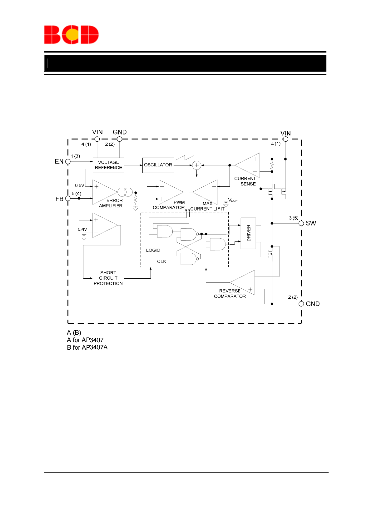
Functional Block Diagram
Figure 3. Functional Block Diagram of AP3407/A
Dec. 2011 Rev. 1. 3 BCD Semiconductor Manufacturing Limited
3
Page 4
Data Sheet
1.2A, 1.4MHz High Efficiency Synchronous DC-DC Buck Converter AP3407/A
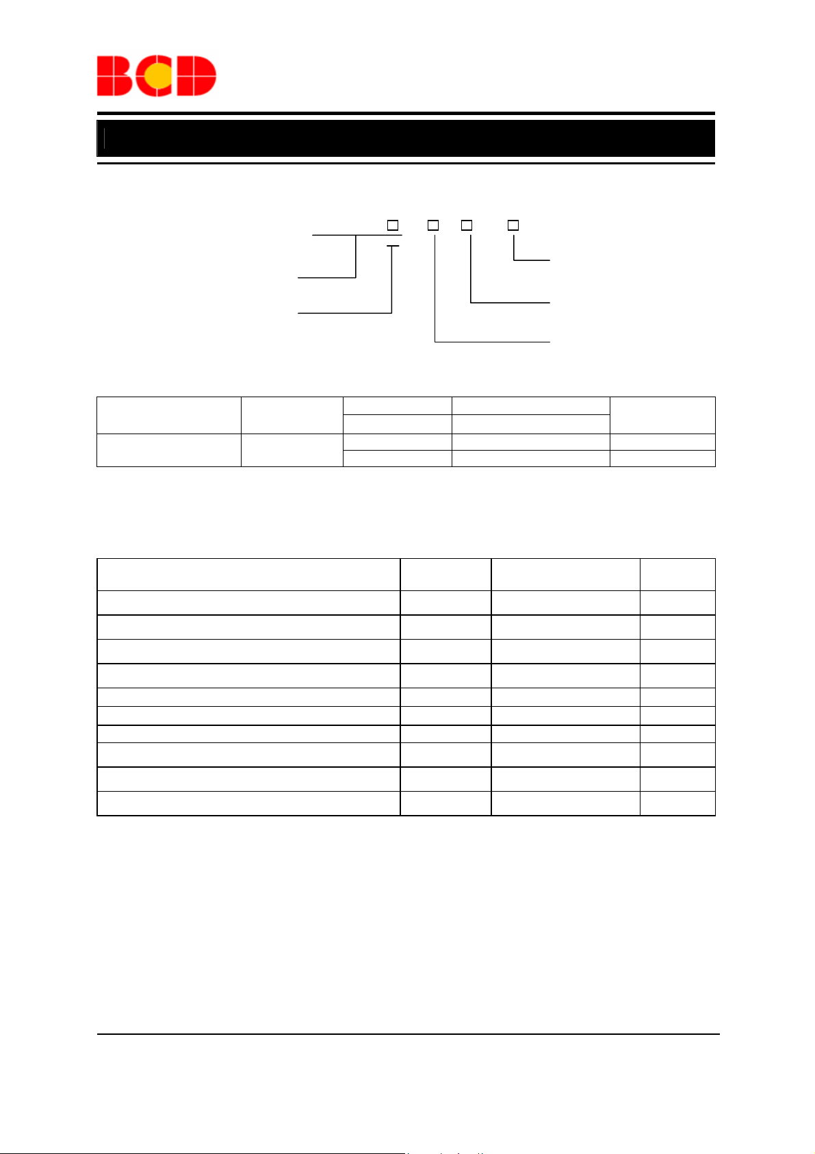
Ordering Information
AP3407 -
G1: Green
Circuit Type
Blank: AP3407
TR: Tape & Reel
A: AP3407A
K: SOT-23-5
Package
SOT-23-5 -40 to 85 ºC
BCD Semiconductor's Pb-free products, as designated with "G1" suffix in the part number, are RoHS compliant
and green.
Temperature
Range
Part Number Marking ID
Green Green
AP3407KTR-G1 GJA Tape & Reel
AP3407AKTR-G1 GJB Tape & Reel
Packing Type
Absolute Maximum Ratings (Note 1)
Parameter Symbol Value Unit
Input Voltage VIN -0.3 to 6.0 V
Feedback Voltage VFB -0.3 to VIN +0.3 V
EN Pin Voltage VEN -0.3 to VIN+0.3 V
SW Pin Voltage VSW -0.3 to VIN+0.3 V
Thermal Resistance
Thermal Resistance
θ
JA
θ
JC
265 ºC/W
60 ºC/W
Power Dissipation PD 0.377 W
Operating Junction Temperature TJ 150 ºC
Storage Temperature T
Lead Temperature (Soldering, 10sec) T
Note 1: Stresses greater than those listed under “Absolute Maximum Ratings” may cause permanent damage to
the device. These are stress ratings only, and functional operation of the device at these or any other conditions
beyond those indicated under “Recommended Operating Conditions” is not implied. Exposure to “Absolute
Maximum Ratings” for extended periods may affect device reliability.
Note 2: The junction temperature rise is given by T
θ
is the thermal resistance from junction of the die to the ambient temperature; The junction temperature, TJ is
JA
given by T
J=TA+TR
, where TA is the ambient temperature.
RISING=PD
-65 to 150 ºC
STG
260 ºC
LEAD
*θJA, where PD is the power dissipated by regulator,
Dec. 2011 Rev. 1. 3 BCD Semiconductor Manufacturing Limited
4
Page 5

Data Sheet
1.2A, 1.4MHz High Efficiency Synchronous DC-DC Buck Converter AP3407/A
Recommended Operating Conditions
Parameter Symbol Min Max Unit
Input Voltage VIN 2.5 5.5 V
Maximum Output Current I
OUT (MAX)
1.2 A
Operating Ambient Temperature TA -40 85 ºC
Electrical Characteristics
VIN=V
DD =VPVDD
Parameters Symbol Conditions Min Typ Max Unit
Input Voltage VIN 2.5 5.5 V
Quiescent Current IQ V
Shutdown Supply Current I
Reference Voltage V
Feedback Bias Current IFB V
Output Voltage Accuracy
PMOSFET RON R
NMOSFET RON R
Switch Current Limit I
=3.3V, TA=25℃, unless otherwise specified.
=0.65V 62 100
FB
V
STBY
REF
∆V
OUT
ISW = 200mA
DS(ON)_ P
ISW = -200mA
DS(ON) _N
LIM
=GND 0.1 1
EN
For Adjustable Output
Voltage
-0.1 0.1
FB=VIN
-2 2 %
=0.55V 1.5 2.0 A
V
FB
µA
µA
0.588 0.6 0.612 V
µA
0.28
0.25
Ω
Ω
VH 1.5
EN Pin Threshold
V
VL 0.4
UVLO Threshold V
VDD Rising 2.3
UVLO
V
UVLO Hysteresis V
Oscillator Frequency f
Max. Duty Cycle D
0.2
HYS
1.12 1.40 1.68 MHz
OSC
VFB=0V 100
MAX
%
Min. Duty Cycle D
N-MOS SW Leakage
Current
V
MIN
V
=6.5V 0
FB
=3.3V, VSW=3.3V 0.1
IN
µA
Soft-start Time t 1 ms
Thermal Shutdown T
Thermal Shutdown
Hysteresis
160 ºC
OTSD
T
20 ºC
HYS
Dec. 2011 Rev. 1. 3 BCD Semiconductor Manufacturing Limited
5
Page 6

Data Sheet
1.2A, 1.4MHz High Efficiency Synchronous DC-DC Buck Converter AP3407/A
Typical Performance Characteristics
100
95
90
85
80
75
70
65
Efficiency (%)
60
55
50
45
40
200 400 600 800 1000 1200
Output Current (mA)
VIN=3.3V
=2.5V
V
OUT
96
88
80
Efficiency (%)
72
23456
Figure 4. Efficiency vs. Output Current
Figure 5. Efficiency vs. Input Voltage
2.51
2.50
2.49
Output Voltage (V)
2.48
2.47
200 400 600 800 1000 1200
Output Current (mA)
VIN=3.3V
V
=2.5V
OUT
1.8
1.7
1.6
1.5
Frequency (MHz)
1.4
1.3
2.5 3.0 3.5 4.0 4.5 5.0 5.5 6.0 6.5
Figure 6. Output Voltage vs. Output Current Figure 7. Frequency vs. Input Voltage
Input Voltage (V)
Input Voltage (V)
V
OUT
I
OUT
=2.5V
I
OUT
I
OUT
=300mA
=0.5A
=1.0A
Dec. 2011 Rev. 1. 3 BCD Semiconductor Manufacturing Limited
6
Page 7

Data Sheet
1.2A, 1.4MHz High Efficiency Synchronous DC-DC Buck Converter AP3407/A
Typical Performance Characteristics (Continued)
1.7
1.6
1.5
1.4
Frequency (MHz)
1.3
1.2
-40 0 40 80 120 160
0.62
Temperature (OC)
VIN=3.3V
V
=2.5V
OUT
0.61
0.60
0.59
Feedback Voltage (V)
0.58
0.57
-40 0 40 80 120 160
Figure 8. Frequency vs. Temperature Figure 9. Feedback Voltage vs. Temperature
VIN=3.3V
Temperature (OC)
2.2
2.0
1.8
1.6
OCP Current Limit (A)
1.4
1.2
-40 0 40 80 120 160
Figure 10. OCP Current Limit vs. Temperature Figure 11. R
Temperature (OC)
VIN=3.3V
V
=0.55V
FB
0.5
0.4
0.3
(Ω)
0.2
DS(ON)-UP
R
0.1
0.0
-40 0 40 80 120 160
Temperature (OC)
DS (ON)_UP
VIN=3.3V
I
=200mA
SW
vs. Temperature
Dec. 2011 Rev. 1. 3 BCD Semiconductor Manufacturing Limited
7
Page 8

Data Sheet
1.2A, 1.4MHz High Efficiency Synchronous DC-DC Buck Converter AP3407/A
Typical Performance Characteristics (Continued)
0.32
0.28
0.24
(Ω)
0.20
DS(ON)-Low
R
0.16
0.12
Figure 12. R
VIN=3.3V
I
=200mA
SW
-40 0 40 80 120 160
Temperature (OC)
DS (ON)_LOW
vs. Temperature
Dec. 2011 Rev. 1. 3 BCD Semiconductor Manufacturing Limited
8
Page 9

Data Sheet
1.2A, 1.4MHz High Efficiency Synchronous DC-DC Buck Converter AP3407/A
T ypical Application
R2 R1
V
IN
EN
VIN
AP3407/A-ADJ
C
IN
F
Figure 13. Typical Application of AP3407/A
FB
GND
V
L
SW
H
2.2
C
OUT
F
OUT
Dec. 2011 Rev. 1. 3 BCD Semiconductor Manufacturing Limited
9
Page 10

Data Sheet
1.2A, 1.4MHz High Efficiency Synchronous DC-DC Buck Converter AP3407/A
Mechanical Dimensions
SOT-23-5 Unit: mm(inch)
2.820(0.111)
0.100(0.004)
0.200(0.008)
0°
8°
0.950(0.037)
Y
T
P
3.020(0.119)
1.800(0.071)
2.000(0.079)
0.300(0.012)
0.400(0.016)
0.200(0.008)
0
0
7
.
0
0
(
.
R
E
F
0
8
2
)
0
.
0
0
.
0
1
.
0
0
(
0
0
9
0
(
0
0
3
.
1
0
)
0
0
.
0
(
0
0
0
.
0
0
5
(
)
6
3
0
.
)
5
.
)
1
5
0
Dec. 2011 Rev. 1. 3 BCD Semiconductor Manufacturing Limited
10
Page 11

BCD Semiconductor Manufacturing Limited
IMPORTANT NOTICE
IMPORTANT NOTICE
BCD Semiconductor Manufacturing Limited reserves the right to make changes without further notice to any products or specifi-
BCD Semiconductor Manufacturing Limited reserves the right to make changes without further notice to any products or specifi-
cations herein. BCD Semiconductor Manufacturing Limited does not assume any responsibility for use of any its products for any
cations herein. BCD Semiconductor Manufacturing Limited does not assume any responsibility for use of any its products for any
particular purpose, nor does BCD Semiconductor Manufacturing Limited assume any liability arising out of the application or use
particular purpose, nor does BCD Semiconductor Manufacturing Limited assume any liability arising out of the application or use
of any its products or circuits. BCD Semiconductor Manufacturing Limited does not convey any license under its patent rights or
of any its products or circuits. BCD Semiconductor Manufacturing Limited does not convey any license under its patent rights or
other rights nor the rights of others.
other rights nor the rights of others.
http://www.bcdsemi.com
MAIN SITE
MAIN SITE
- Headquarters
BCD Semiconductor Manufacturing Limited
BCD Semiconductor Manufactur ing Limited
- Wafer Fab
No. 1600, Zi Xing Road, Shanghai ZiZhu Science-based Industrial Park, 200241, China
Shanghai SIM-BCD Semiconductor Manufacturing Limited
Tel: +86-21-24162266, Fax: +86-21-24162277
800, Yi Shan Road, Shanghai 200233, China
Tel: +86-21-6485 1491, Fax: +86-21-5450 0008
REGIONAL SALES OFFICE
Shenzhen Office
REGIONAL SALES OFFICE
Shanghai SIM-BCD Semiconductor Manufacturing Co., Ltd., Shenzhen Office
Shenzhen Office
Unit A Room 1203, Skyworth Bldg., Gaoxin Ave.1.S., Nanshan District, Shenzhen,
Shanghai SIM-BCD Semiconductor Manufacturing Co., Ltd. Shenzhen Office
China
Advanced Analog Circuits (Shanghai) Corporation Shenzhen Office
Tel: +86-755-8826 7951
Room E, 5F, Noble Center, No.1006, 3rd Fuzhong Road, Futian District, Shenzhen 518026, China
Fax: +86-755-8826 7865
Tel: +86-755-8826 7951
Fax: +86-755-8826 7865
- Wafer Fab
BCD Semiconductor Manufacturing Limited
Shanghai SIM-BCD Semiconductor Manufacturing Co., Ltd.
- IC Design Group
800 Yi Shan Road, Shanghai 200233, China
Advanced Analog Circuits (Shanghai) Corporation
Tel: +86-21-6485 1491, Fax: +86-21-5450 0008
8F, Zone B, 900, Yi Shan Road, Shanghai 200233, China
Tel: +86-21-6495 9539, Fax: +86-21-6485 9673
Taiwan Office
BCD Semiconductor (Taiwan) Company Limited
Taiwan Office
4F, 298-1, Rui Guang Road, Nei-Hu District, Taipei,
BCD Semiconductor (Taiwan) Company Limited
Tai wan
4F, 298-1, Rui Guang Road, Nei-Hu District, Taipei,
Tel: +886-2-2656 2808
Taiwan
Fax: +886-2-2656 2806
Tel: +886-2-2656 2808
Fax: +886-2-2656 2806
USA Office
BCD Semiconductor Corp.
USA Office
30920 Huntwood Ave. Hayward,
BCD Semiconductor Corporation
CA 94544, USA
30920 Huntwood Ave. Hayward,
Tel : +1-510-324-2988
CA 94544, U.S.A
Fax: +1-510-324-2788
Tel : +1-510-324-2988
Fax: +1-510-324-2788
 Loading...