

Page 1
1.1MHz, 800mA SYNCHRONOUS DC-DC BUCK CONVERTER AP3406A
Data Sheet
General Description
The AP3406A is a 1.1MHz fixed frequency, current
mode, PWM synchronous buck (step-down) DC-DC
converter, capable of driving a 800mA load with high
efficiency, excellent line and load regulation. The
device integrates a main switch and a synchronous
switch without an external Schottky diode. It is ideal
for powering portable equipment that runs from a
single Li-ion battery.
A standard series of inductors are available from
several different manufacturers optimized for use
with the AP3406A. This feature greatly simplifies the
design of switch-mode power supplies.
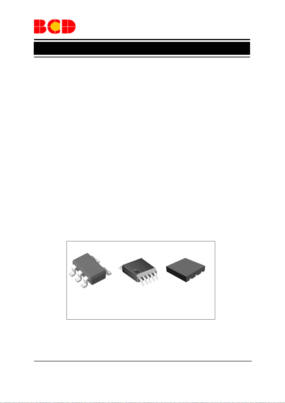
This IC is available in TSOT-23-5, MSOP-10 and
DFN-2×2-6(1) packages.
Features
High Efficiency: up to 95%
•
• Output Current: 800mA
• Input Voltage Range: 2.5V to 5.5V
• Fixed 1.1MHz Frequency
• Current Mode Control
• 100% Duty Cycle in Dropout
• Built-in Short Circuit Protection
• Built-in Thermal Shutdown Function
• Built-in Current Limit Function
• Shutdown Current: <1µA
Applications
• GPS
• WiFi Card
• Portable Media Player
• Digital Still and Video Cameras
TSOT-23-5 MSOP-10 DFN-2×2-6(1)
Figure 1. Package Types of AP3406A
Feb. 2013 Rev. 1. 5 BCD Semiconductor Manufacturing Limited
1
Page 2
Data Sheet
1.1MHz, 800mA SYNCHRONOUS DC-DC BUCK CONVERTER AP3406A
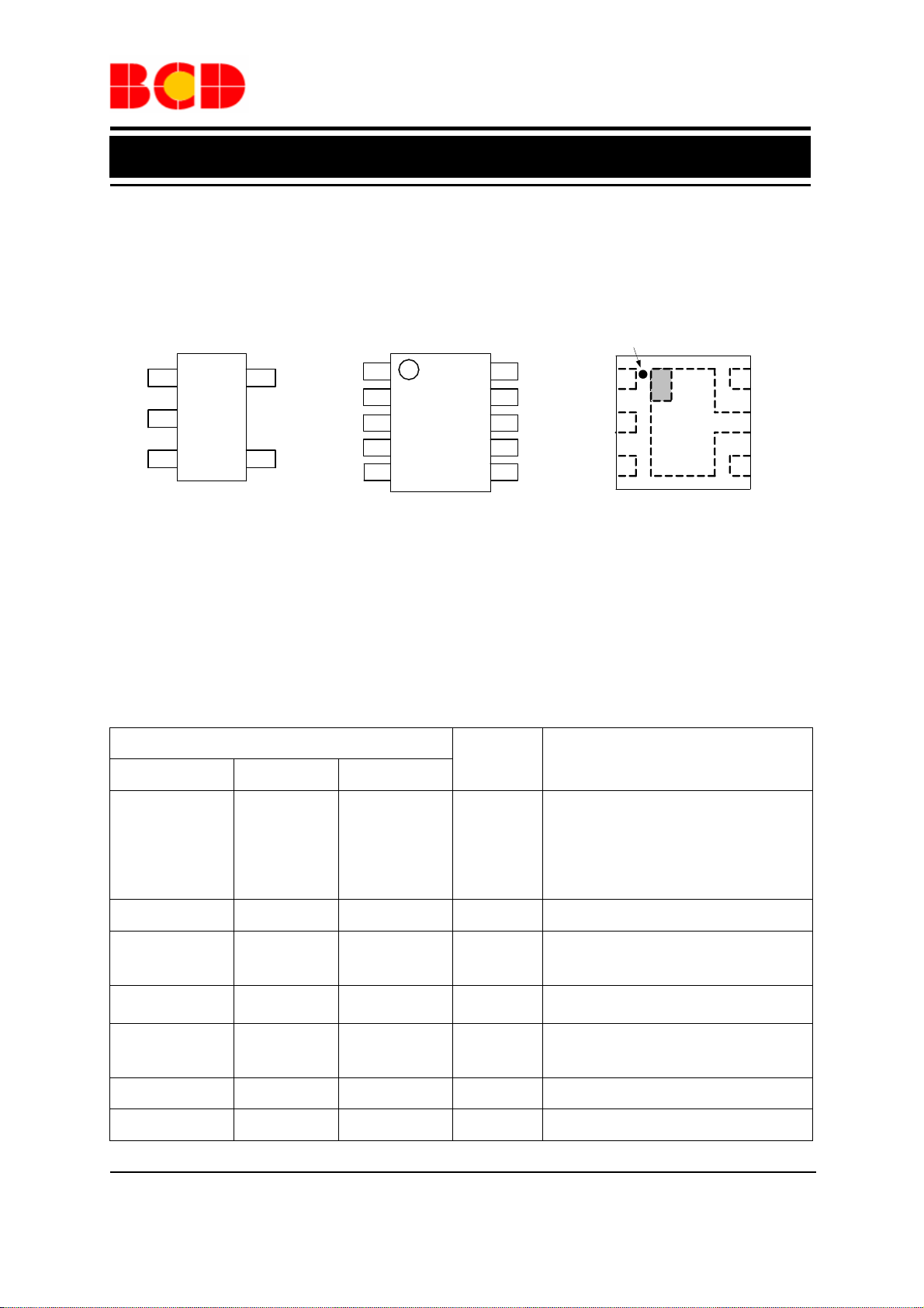
Pin Configuration
KT Package MM Package DN Package
TSOT-23-5 MSOP-10 DFN-2×2-6(1)
P in 1 Mark
EN
GND
1
2
5
SW
34
FB
VIN
VIN
NC
GND
NC
FB
1
2
3
4
5
10
Figure 2. Pin Configuration of AP3406A (Top View)
Pin Description
Pin Number
Pin Name Function
TSOT-23-5 MSOP-10 DFN-2×2-6(1)
1 8 2 EN
2 3 5 GND Ground pin
3 9 4 SW
4 1 3 VIN
5 5 6 FB
2, 4, 6, 7 1 NC No connection
PGND
9
SW
8
EN
NC
7
6
NC
NC
EN
VIN
1
2
3
6
FB
GND
5
4
SW
Control input pin. Forcing this pin above
1.5V enables the IC. Forcing this pin
below 0.6V shuts down the IC. When
the IC is in shutdown mode, all
functions are disabled to decrease the
supply current below 1µA
Power switch output pin. Inductor
connection to drain of the internal PFET
and NFET switches
Supply input pin. Bypass to GND with a
10µF or greater ceramic capacitor
Feedback pin. Connect it with an
external resistor divider network to
program the system output voltage
10 PGND Power ground pin
Feb. 2013 Rev. 1. 5 BCD Semiconductor Manufacturing Limited
2
Page 3
Data Sheet
1.1MHz, 800mA SYNCHRONOUS DC-DC BUCK CONVERTER AP3406A
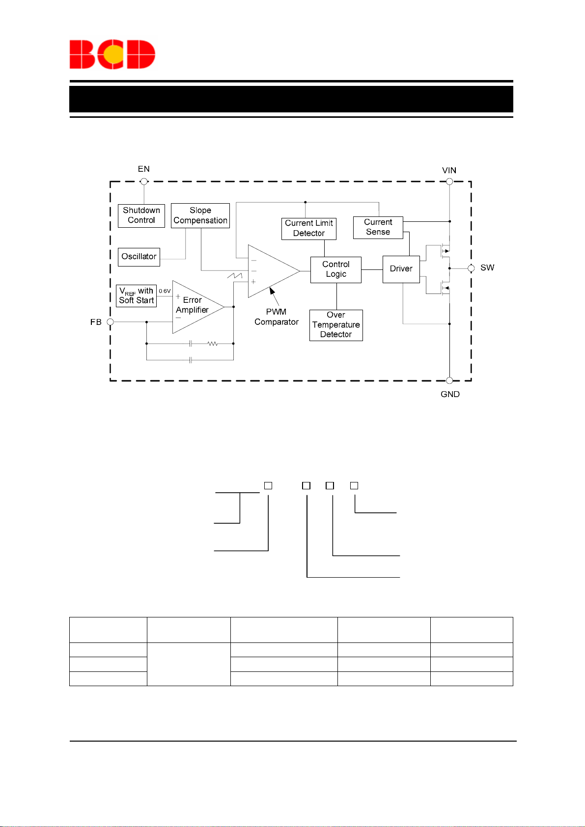
Functional Block Diagram
Figure 3. Functional Block Diagram of AP3406A
Ordering Information
AP3406A -
Circuit Type
Package
KT: TSOT-23-5
MM: MSOP-10
DN: DFN-2×2-6(1)
Package
TSOT-23-5
MSOP-10 AP3406AMM-ADJTRG1 3406AMM-G1 Tape & Reel
DFN-2×2-6(1) AP3406ADN-ADJTRG1 BA Tape & Reel
Temperature
Range
-40 to 85°C
Part Number Marking ID Packing Type
AP3406AKT-ADJTRG1 L2A Tape & Reel
BCD Semiconductor's Pb-free products, as designated with "G1" suffix in the part number, are RoHS
compliant and green.
G1: Green
TR: Tape & Reel
ADJ: Adjustable Voltage
Feb. 2013 Rev. 1. 5 BCD Semiconductor Manufacturing Limited
3
Page 4
Data Sheet
1.1MHz, 800mA SYNCHRONOUS DC-DC BUCK CONVERTER AP3406A
Absolute Maximum Ratings (Note 1)
Parameter Symbol Value Unit
Input Voltage VIN -0.3 to 6 V
Feedback Voltage VFB -0.3 to VIN +0.3 V
EN Pin Voltage VEN -0.3 to VIN+0.3 V
SW Pin Voltage VSW -0.3 to VIN+0.3 V
TSOT-23-5 250
Thermal Resistance
Operating Junction Temperature TJ 150 ºC
Storage Temperature T
Lead Temperature (Soldering, 10sec) T
θ
JA
-65 to 150 ºC
STG
260 ºC
LEAD
MSOP-10 135
DFN-2×2-6(1) 100
ºC/W
Note 1: Stresses greater than those listed under “Absolute Maximum Ratings” may cause permanent damage to
the device. These are stress ratings only, and functional operation of the device at these or any other conditions
beyond those indicated under “Recommended Operating Conditions” is not implied. Exposure to “Absolute
Maximum Ratings” for extended periods may affect device reliability.
Recommended Operating Conditions
Parameter Symbol Min Max Unit
Input Voltage VIN 2.5 5.5 V
Maximum Output Current I
Operating Ambient Temperature TA -40 85 ºC
OUT (MAX)
800 mA
Feb. 2013 Rev. 1. 5 BCD Semiconductor Manufacturing Limited
4
Page 5

Data Sheet
1.1MHz, 800mA SYNCHRONOUS DC-DC BUCK CONVERTER AP3406A
Electrical Characteristics
V
IN =VEN
operating temperature range from -40 to 85ºC.
Parameters Symbol Conditions Min Typ Max Unit
Supply Current ICC VFB=0.55V 400 600
=3.6V, T
=25℃, unless otherwise specified. Specifications with boldface type apply over full
A
µA
Shutdown Supply Current I
Under Voltage Lockout
Threshold
Under Voltage Lockout
Hysteresis
VEN=0V, VIN=5.5V 0.01 1
SHDN
V
UVLO
V
HUVLO
Rising edge 2.27 V
200 mV
µA
Feedback Bias Current IFB VFB=0.65V -50 0.5 50 nA
Feedback Voltage VFB I
Maximum Output Current
I
OUT (MAX)
=100mA
OUT
V
=2.5V,
IN
V
OUT
VIN=3.6V,
V
OUT
VIN=4.6V,
V
OUT
Switch Current Limit I
Oscillator Frequency f
EN Pin Threshold
EN Pin Input Leakage
Current
Internal PFET On
Resistance
Internal NFET On
Resistance
Maximum Duty Cycle D
Soft-start Time TSS
Thermal Shutdown
Threshold
Thermal Shutdown
Hysteresis
VFB=0.55V 0.95 1.25 A
LIM
0.8 1.1 1.4 MHz
OSC
V
0.6
ENL
V
1.5
ENH
I
VEN=3.6V -0.1 0.1
H
IL VEN=0V -0.1 0.1
R
ISW=100mA 0.44 Ω
DSONP
R
ISW=-100mA 0.29 Ω
DSONN
VFB=0.55V 100 %
MAX
=0V to V
V
EN
I
=50mA
OUT
T
160 ºC
OTSD
T
30 ºC
HYS
=0.9V
=1.2V
=3.3V
IN
0.588/
0.582
0.600
800
800
800
220
0.612/
0.618
V
mA
V
µA
µA
µs
Feb. 2013 Rev. 1. 5 BCD Semiconductor Manufacturing Limited
5
Page 6

Data Sheet
1.1MHz, 800mA SYNCHRONOUS DC-DC BUCK CONVERTER AP3406A
Typical Performance Characteristics
L=10µH, CIN=C
=10µF, TA=25oC, unless otherwise noted.
OUT
1.4
1.3
1.2
1.1
1.0
0.9
0.8
2.0 2.5 3.0 3.5 4.0 4.5 5.0 5.5 6.0
Input Voltage (V)
Figure 4. Frequency vs. Input Voltage
2.0
1.8
1.6
1.4
1.2
1.0
0.8
0.6
0.4
0.2
0.0
-60 -40 -20 0 20 40 60 80 100
Temperature (OC)
Figure 6. Current Limit vs. Temperature Figure 7. Output Voltage vs. Output Current
Frequency (MHz)
Current Limit (A)
VIN=3.6V
V
=1.8V
OUT
I
=0A
OUT
VIN=3.6V
VFB=0.55V
0.7
0.6
0.5
0.4
Supply Current (mA)
0.3
0.2
-60 -40 -20 0 20 40 60 80 100 120 140 160
Figure 5. Supply Current vs. Temperature
2.0
1.8
1.6
1.4
1.2
1.0
0.8
Output Voltage (V)
0.6
0.4
0.2
0.0
0.00.20.40.60.81.01.21.4
VIN=3.6V
V
=1.8V
OUT
VIN=3.6V
VFB=0.55V
Temperature (oC)
Output Current (A)
Feb. 2013 Rev. 1. 5 BCD Semiconductor Manufacturing Limited
6
Page 7

Data Sheet
1.1MHz, 800mA SYNCHRONOUS DC-DC BUCK CONVERTER AP3406A
Typical Performance Characteristics (Continued)
VSW
2V/div
V
OUT
20mV/div
400ns/div
400ns/div 400ns/div
Figure 8. Light Load Operation Figure 9. Heavy Load Operation
(VIN=3.6V, V
OUT
=1.8V, I
=0mA) (VIN=3.6V, V
OUT
V
SW
2V/div
V
OUT
20mV/div
OUT
=1.8V, I
=800mA)
OUT
500mA/div
100mV/div
I
OUT
V
OUT
(V
=3.6V, V
IN
I
V
OUT
2V/div
V
2V/div
IN
EN
=1.8V, R
OUT
LOAD
=2.5Ω)
500mA/div
200µs/div 400µs/div
Figure 10. Load Transient Figure 11. Start up from Shutdown
OUT
=1.8V, I
=0mA to 800mA) (VIN=3.6V, V
OUT
Feb. 2013 Rev. 1. 5 BCD Semiconductor Manufacturing Limited
7
Page 8

Data Sheet
1.1MHz, 800mA SYNCHRONOUS DC-DC BUCK CONVERTER AP3406A
Typical Performance Characteristics (Continued)
V
OUT
1V/div
V
SW
2V/div
IL
1A/div
V
OUT
1V/div
V
SW
2V/div
1A/div
I
L
10µs/div 40µs/div
Figure 12. Short Circuit Protection Figure 13. Short Circuit Recovery
(V
=3.6V, V
IN
=1.8V, no load) (VIN=3.6V, V
OUT
=1.8V, no load)
OUT
1.0
0.9
0.8
0.7
0.6
0.5
0.4
Efficiency (%)
0.3
0.2
0.1
0.0
TSOT-23-5
MSOP-10
0.1 1
Output Current (A)
VIN=3.6V
V
=1.8V
OUT
L=10µH
1.0
0.9
0.8
0.7
0.6
0.5
0.4
Efficiency (%)
0.3
0.2
0.1
0.0
TSOT-23-5
MSOP-10
0.1 1
Output Current (A)
VIN=4.2V
V
=3.3V
OUT
L=10µH
Figure 14. Efficiency vs. Output Current Figure 15. Efficiency vs. Output Current
Feb. 2013 Rev. 1. 5 BCD Semiconductor Manufacturing Limited
8
Page 9

Data Sheet
1.1MHz, 800mA SYNCHRONOUS DC-DC BUCK CONVERTER AP3406A
Typical Performance Characteristics (Continued)
2.0
1.5
1.0
0.5
0.0
-0.5
-1.0
-1.5
Normalized Feedback Voltage (%)
-2.0
-60 -40 -20 0 20 40 60 80 100
Temperature (oC)
VIN=3.6V
V
=1.8V
OUT
Figure 16. Normalized Feedback Voltage vs. Temperature
T ypical Application
R2
V
IN
2.5V to 5.5V
C
IN
10µF
EN
VIN
AP3406A-ADJ
Figure 17. Typical Application of AP3406A
FB
GND
SW
300k150k
R1
L
10µH
C
OUT
10µF
V
OUT
1.8V
800mA
Feb. 2013 Rev. 1. 5 BCD Semiconductor Manufacturing Limited
9
Page 10

Data Sheet
1.1MHz, 800mA SYNCHRONOUS DC-DC BUCK CONVERTER AP3406A
Mechanical Dimensions
TSOT-23-5 Unit: mm(inch)
5
°
GAUGE PLANE
Feb. 2013 Rev. 1. 5 BCD Semiconductor Manufacturing Limited
10
Page 11

Data Sheet
1.1MHz, 800mA SYNCHRONOUS DC-DC BUCK CONVERTER AP3406A
Mechanical Dimensions (Continued)
MSOP-10 Unit: mm(inch)
Feb. 2013 Rev. 1. 5 BCD Semiconductor Manufacturing Limited
11
Page 12

Data Sheet
1.1MHz, 800mA SYNCHRONOUS DC-DC BUCK CONVERTER AP3406A
Mechanical Dimensions (Continued)
DFN-2×2-6(1) Unit: mm(inch)
0.224(0.009)
0.376(0.015)
1.900(0.075)
2.100(0.083)
0.200(0.008)
MIN.
0.650(0.026)
TYP.
N4 N5 N6
0.250(0.010)
0.350(0.014)
0.550(0.022)
0.650(0.026)
Pin 1 Mark
0.000(0.000)
0.050(0.002)
0.152(0.006)
REF.
1.900(0.075)
2.100(0.083)
1.500(0.059)
1.700(0.067)
12
2
N2N3
DETAIL A
Pin 1 options
0.850(0.033)
1.050(0.041)
PIN #1 IDENTIFICATION
See DETAIL A
N1
1
1
2
Feb. 2013 Rev. 1. 5 BCD Semiconductor Manufacturing Limited
12
Page 13

BCD Semiconductor Manufacturing Limited
IMPORTANT NOTICE
IMPORTANT NOTICE
BCD Semiconductor Manufacturing Limited reserves the right to make changes without further notice to any products or specifi-
BCD Semiconductor Manufacturing Limited reserves the right to make changes without further notice to any products or specifi-
cations herein. BCD Semiconductor Manufacturing Limited does not assume any responsibility for use of any its products for any
cations herein. BCD Semiconductor Manufacturing Limited does not assume any responsibility for use of any its products for any
particular purpose, nor does BCD Semiconductor Manufacturing Limited assume any liability arising out of the application or use
particular purpose, nor does BCD Semiconductor Manufacturing Limited assume any liability arising out of the application or use
of any its products or circuits. BCD Semiconductor Manufacturing Limited does not convey any license under its patent rights or
of any its products or circuits. BCD Semiconductor Manufacturing Limited does not convey any license under its patent rights or
other rights nor the rights of others.
other rights nor the rights of others.
http://www.bcdsemi.com
MAIN SITE
MAIN SITE
- Headquarters
BCD Semiconductor Manufacturing Limited
BCD Semiconductor Manufactur ing Limited
- Wafer Fab
No. 1600, Zi Xing Road, Shanghai ZiZhu Science-based Industrial Park, 200241, China
Shanghai SIM-BCD Semiconductor Manufacturing Limited
Tel: +86-21-24162266, Fax: +86-21-24162277
800, Yi Shan Road, Shanghai 200233, China
Tel: +86-21-6485 1491, Fax: +86-21-5450 0008
REGIONAL SALES OFFICE
Shenzhen Office
REGIONAL SALES OFFICE
Shanghai SIM-BCD Semiconductor Manufacturing Co., Ltd., Shenzhen Office
Shenzhen Office
Unit A Room 1203, Skyworth Bldg., Gaoxin Ave.1.S., Nanshan District, Shenzhen,
Shanghai SIM-BCD Semiconductor Manufacturing Co., Ltd. Shenzhen Office
China
Advanced Analog Circuits (Shanghai) Corporation Shenzhen Office
Tel: +86-755-8826 7951
Room E, 5F, Noble Center, No.1006, 3rd Fuzhong Road, Futian District, Shenzhen 518026, China
Fax: +86-755-8826 7865
Tel: +86-755-8826 7951
Fax: +86-755-8826 7865
- Wafer Fab
BCD Semiconductor Manufacturing Limited
Shanghai SIM-BCD Semiconductor Manufacturing Co., Ltd.
- IC Design Group
800 Yi Shan Road, Shanghai 200233, China
Advanced Analog Circuits (Shanghai) Corporation
Tel: +86-21-6485 1491, Fax: +86-21-5450 0008
8F, Zone B, 900, Yi Shan Road, Shanghai 200233, China
Tel: +86-21-6495 9539, Fax: +86-21-6485 9673
Taiwan Office
BCD Semiconductor (Taiwan) Company Limited
Taiwan Office
4F, 298-1, Rui Guang Road, Nei-Hu District, Taipei,
BCD Semiconductor (Taiwan) Company Limited
Tai wan
4F, 298-1, Rui Guang Road, Nei-Hu District, Taipei,
Tel: +886-2-2656 2808
Taiwan
Fax: +886-2-2656 2806
Tel: +886-2-2656 2808
Fax: +886-2-2656 2806
USA Office
BCD Semiconductor Corp.
USA Office
30920 Huntwood Ave. Hayward,
BCD Semiconductor Corporation
CA 94544, USA
30920 Huntwood Ave. Hayward,
Tel : +1-510-324-2988
CA 94544, U.S.A
Fax: +1-510-324-2788
Tel : +1-510-324-2988
Fax: +1-510-324-2788
 Loading...