

Page 1
AP331A
SINGLE DIFFERENTIAL COMPARATOR
Features
• Wide supply
Voltage range: 2.0V to 36V
Single or dual supplies: ±1.0V to ±18V
• Very low supply current drain (0.4mA) – independent of
supply voltage
• Low input biasing curr ent: 150nA
• Low input offset current: ±70nA
• Low input offset voltage: ±4mV
• Input common-mode voltage ra nge includes ground
• Differential input voltage range equal to the power
supply voltage
• Low output saturation voltage: 250mV at 4mA
• Output voltage compatible with TTL, DTL, ECL, MOS
and CMOS logic systems
• SOT25 and SOT25R: Available in “Green” Molding
Compound (No Br, Sb)
• Lead Free Finish/ RoHS Compliant ( Note 1)
Applications
• High precision comparators
• Reduced V
• Eliminates need for dual supplies
• Allows sensing near ground
• Compatible with all forms of logic
• Power drain suitable for battery operation
drift over temperature
OS
Ordering Information
General Description
The AP331A is a precision voltage comparators with an offset
voltage specification as low as 8.0 mV max for comparator which
were designed specifically to operate from a single power supply
over a wide range of voltages. Operation from split power
supplies is also possible and the low power supply current drain
is independent of the magnitude of the pow er sup ply voltage. Th e
comparator also have a unique characteristic in that the input
common-mode voltage range includes ground, even though
operated from a single power supply voltage.
Application areas include limit comparators, simple analog to
digital converters; pulse, square wave and time delay gene rators;
wide range VCO; MOS clock timers; multivibrators and high
voltage digital logic gates. The AP331A is designed to directly
interface with TTL and CMOS. When operated from both plus
and minus power supplies, the AP331A will directly interface with
MOS logic where their low power drain is a distinct advantage
over standard comparators.
AP331A XX G - 7
Package
W : SOT25
Lead Free
G : Green
WR : SOT25R
Device
AP331AWG-7
AP331AWRG-7
Notes: 1. EU Directive 2002/95/EC (RoHS). All applicable RoHS exemptions applied. Please visit our website at
http://www.diodes.com/products/lead_free.html
2. Pad layout as shown on Diodes Inc. suggested pad layout document AP02001, which can be found on our website at
http://www.diodes.com/datasheets/ap02001.pdf
Package
Code
W SOT25
WR SOT25R
AP331A Rev. 2 1 of 13 FEBRUARY 2009
Packaging
(Note 2)
Quantity Part Number Suffix
3000/Tape & Reel -7
3000/Tape & Reel -7
.
.
www.diodes.com © Diodes Incorporated
Packing
7 : Tape & Reel
7” Tape and Reel
Page 2
SINGLE DIFFERENTIAL COMPARATOR
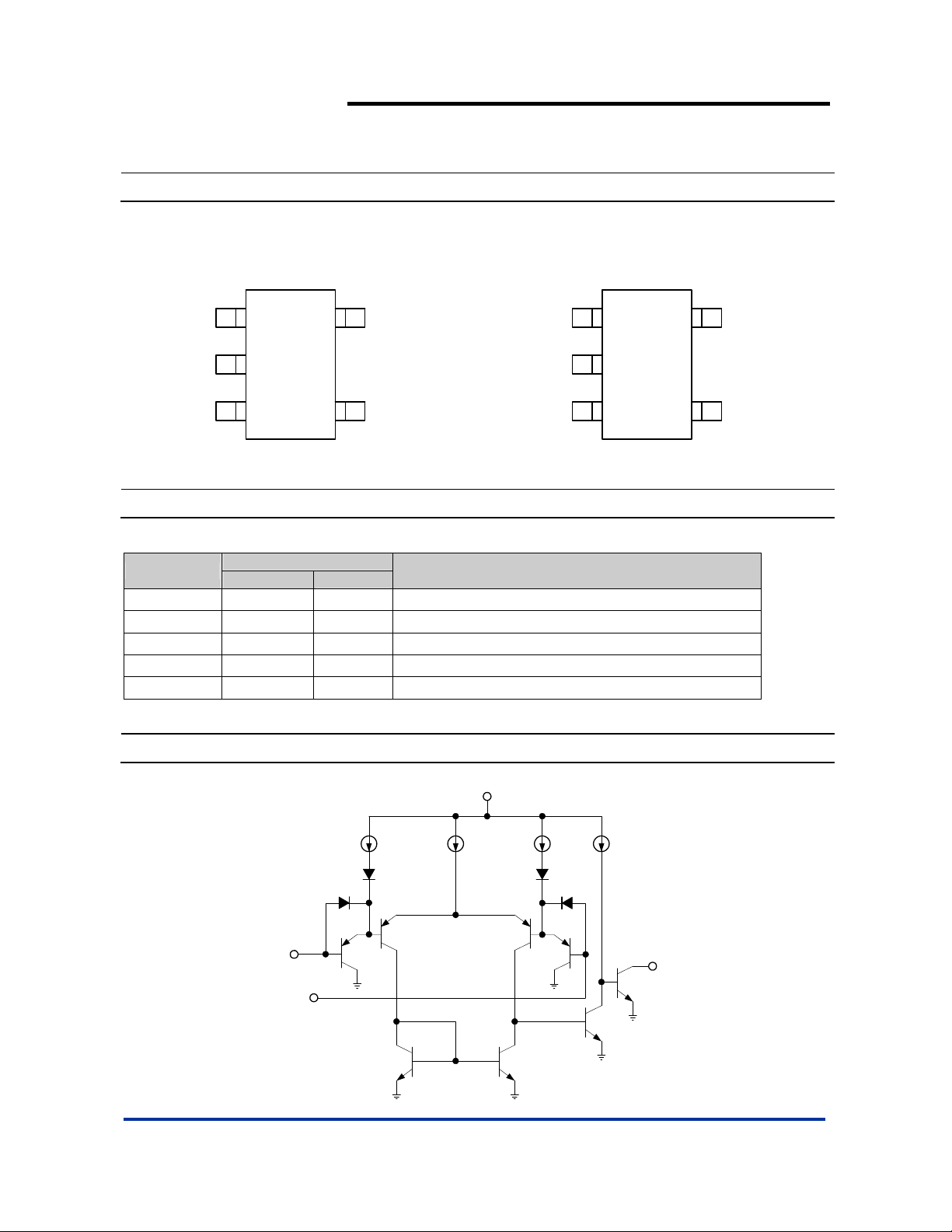
Pin Assignments
(1) SOT25 (2) SOT25R
( Top View )
AP331A
( Top View )
IN-
1
GND
2
IN+
5
43
Vcc
Output
Pin Descriptions
Pin Name
IN- 1 3 Input-
GND 2 2 Ground
IN+ 3 1 Input+
Output 4 4 Output
Vcc 5 5 Power Supply
SOT25
Pin No.
SOT25R
Block Diagram
IN+
1
GND
2
IN-
Description
5
43
Vcc
Output
+
V
100μA3.5μA100μA3.5μA
Q2 Q3
+INPUT
-INPUT
AP331A Rev. 2 2 of 13 FEBRUARY 2009
Q1
Q4
Q6
Q7Q8
www.diodes.com © Diodes Incorporated
OUTPUT
Q5
Page 3
r
r
(+)
(-)
AP331A
SINGLE DIFFERENTIAL COMPARATOR
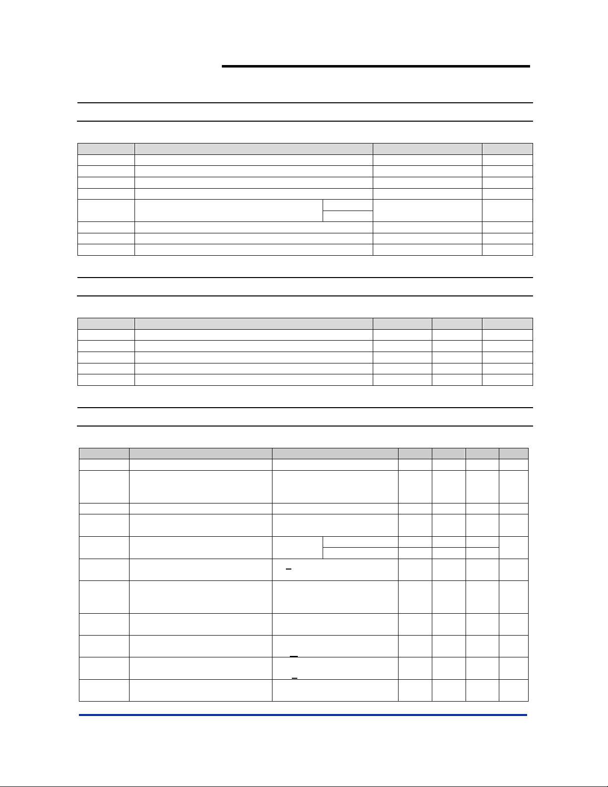
Absolute Maximum Ratings
Symbol Paramete
VCC Supply Voltage 40 V
VIN
Differential Input Voltage (Note 10)
VIN Input Voltage -0.3 to +40 V
ICC
PD
Input Current (V
Power Dissipation (Note 3)
-0.3V) (Note 5)
IN
SOT25
SOT25R
Output Short-Circuit to Ground (Note 4) Continuous
TJ Operating Junction T emperature Range+150
TST Storage Temperature Range -65 to +150
Recommended Operating Conditions
Symbol Paramete
VCC Supply Voltage (Single) +2 +36 V
VCC Supply Voltage (Dual Supplies, V+ VS GND) ±1 ±18 V
VIN
VIN
Differential Input Voltage (Single) (Note 10)
Differential Input Voltage (Dual Supplies) (Note 10)
TA Operating Ambient Temperature 0 70
Electrical Characteristics
= 5V, T
(V
CC
Symbol Parameter Conditions Min Typ. Max Unit
V
OFFSET
I
BIAS
I
OFFSET
ICC Supply Current RL = ∞
I
O(Sink)
V
SAT
I
O(Leak)
AP331A Rev. 2 3 of 13 FEBRUARY 2009
= 25oC, unless otherwise stated)
A
Input Offset Voltage
Input Bias Current
Input Offset Current I
Input Common Mode Voltage
Range
Voltage Gain
Large Signal Response Time
Response Time
Output Sink Current
Saturation Voltage
Output Leaka ge Current
(Note 11)
I
(+) or IIN(-) with Output In
IN
Linear Range, V
CM
= 0V
(Note 7)
-I
V
IN
IN
+
= 30V (Note 8)
V
= 0V - 70 150 nA
CM
+
= 5V - 0.4 1
V
V+ = 36V - 1 2. 5
R
> 15kΩ, V+ = 15V
L
V
= 1V to 11V
O
= TTL Logic Swing,
V
IN
V
= 1.4V, V
REF
R
= 5.1kΩ
L
= 5V, RL = 5.1kΩ
V
RL
= 5V,
RL
(Note 9)
V
(-) = 1V, VIN(+) = 0,
IN
< 1.5V
V
O
V
(-) = 1V, VIN(+) = 0,
IN
< 4mA
I
SINK
V
(-) = 0, VIN(+) = 1V,
IN
= 5V
V
O
www.diodes.com © Diodes Incorporated
Rating Unit
40 V
50 mA
740 mW
o
C
o
C
Min Max Unit
0 ±36 V
-18 +18 V
o
C
- 4.0 8.0 mV
- 150 400 nA
0 - V
+
-1.5 V
mA
50 200 - V/mV
- 300 - ns
- 1.3 - μs
6.0 16 - mA
- 250 400 mV
- 0.1 - nA
Page 4
(+)
(-)
A
T
AP331A
SINGLE DIFFERENTIAL COMPARATOR
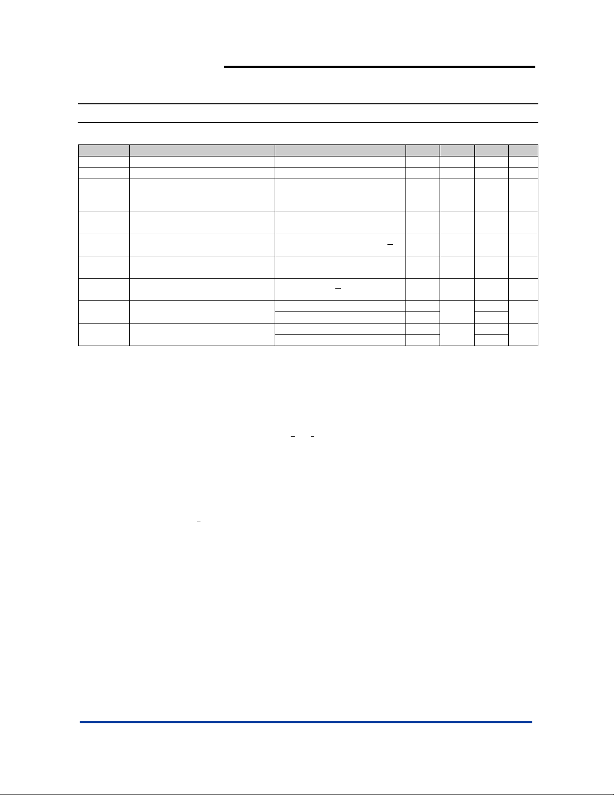
Electrical Characteristics
( V
= 5V ) ( Note 6 )
CC
Symbol Parameter Conditions Min Typ. Max Unit
V
Input Offset Voltage (Note 11) - - 9 mV
OFFSET
I
Input Offset Current I
OFFSET
I
Input Bias Current
BIAS
Input Common Mode Voltage
Range
V
Saturation Voltage
SAT
I
Output Leakage Current
O(Leak)
Differential Input Voltage
θ
θ
Notes: 3. The maximum power dissipation is a function of T
4. Short circuits from the output to V
5. This input current will only exist when the voltage at any of the input leads is driven negative. It is due to the collector-base
junction of the input PNP transistors becoming forward biased and thereby acting as input diode clamps. In addition to this
di ode actio n, there is also lateral NP N parasitic transist or acti on o n the IC chip. This transistor action can cause the output
6. The AP331A temperature specifications are limited to 0°C <
7. The direction of the input current is out of the IC due to the PNP input stage. This current is essentially constant, independent
8. The input common-mode voltage or either input signal voltage should not be allowed to go negative by more than 0.3V. The
9. The response time specified is for a 100mV input step with 5mV overdrive. For larger overdrive signals 300ns can be
10. Positive excursions of input voltage may exceed the power supply level. As long as the other voltage remains within the
11. At output switch point, V
12. Test condition for SOT25 and sot25R: Device mounted on FR-4 substrate PC board, 2oz copper, with minimum recommended pad layout.
Thermal Resistance
JA
Junction-to-Ambient
hermal Resistance
JC
Junction-to-Case
P
= (T
D
ground, the maximum output current is approximately 20mA independent of the magnitude of V
voltages of the comparators to go to the V
is driven negative. This is not destructive and normal output states will re-establish when the input voltage, which is negative,
again returns to a value greater than -0.3V.
of the state of the output so no loading change exists on the reference or input lines.
upper end of the common-mode voltage range is V
independent of the magnitude of V
obtained, see typical performance characteristics section.
common-mode range, the comparator will provide a proper output state. The low input voltage state must not be less than
-0.3V (or 0.3V below the magnitude of the negative power supply, if used).
at 25°C.
-TA)/ θJA . All numbers apply for packages soldered directly onto a PC board.
J(MAX)
+
can cause excessive heating and eventual destruction. When considering short circuits to
+
.
~ 1.4V, RS=0Ω with V+ from 5V to 30V; and over the full input common-mode range (0V to V+-1.5V),
O
J(MAX)
+
voltage level (or to ground for a large overdrive) for the time duration that an input
-I
, V
IN
IN
(+) or IIN(-) with Output In
I
IN
Linear Range, V
= 0V - - 200 n
CM
CM
= 0V
- - 500 nA
(Note 7)
+
=30V (Note 8)
V
(-) = 1V, VIN(+) = 0, I
V
IN
SINK
<
4mA
V
(-) = 0, VIN(+) = 1V,
IN
V
= 30V
O
Keep All V
’s > 0V (or V-, if
IN
Used), (Note 10)
SOT25 (Note 12)
SOT25R (Note 12)
SOT25 (Note 12)
SOT25R (Note 12)
, θJA. The maximum allowable power dissipation at any ambient temperature is
TOP < +70°C.
+
-1.5V at 25°C, but either or both inputs can go to 36V without damage,
0 - V
- - 700 mV
- - 1.0 μA
- - 36 V
173
37
+
.
+
-2.0 V
o
C/W
o
C/W
AP331A Rev. 2 4 of 13 FEBRUARY 2009
www.diodes.com © Diodes Incorporated
Page 5

AP331A
SINGLE DIFFERENTIAL COMPARATOR
Application Information
The AP331A is high gain, wide bandwidth devices, like most comparators, can easily oscillate if the output lead is inadvertently
allowed to capacitively couple to the inputs via stray capacitance. This shows up only during the output voltage transition intervals as the
comparator change states. Power supply bypassing is not required to solve this problem. Standard PC board layout is helpful as it
reduces stray input-output coupling. Reducing the input resistors to < 10kΩ reduces the feedback signal levels and finally, adding even a
small amount (1.0 to 10 mV) of positive feedback (hysteresis) causes such a rapid transition that oscillations due to stray feedback are
not possible. Simply socketing the IC and attaching resistors to the pins will cause input-output oscillations during the small transition
intervals unless hysteresis is used. If the input signa l is a pulse wav eform, with relativ ely fast rise and fall time s, hystere sis is not required.
All input pins of any unused comparators should be tied to the negative supply.
The bias network of the AP331A establishes a drain current independent of the magnitude of the power supply voltage over the
range of from 2.0 V
The differential input voltage may be larger than V+ without damaging the device (Note 10). Protection should be provided to
prevent the input voltages from going negative more than -0.3 V
applications section.
The output of the AP331A is the uncommitted collector of a grounded-emitter NPN output transistor. Many collectors can be tied
together to provide an output OR’ing function. An output pull-up resistor can be connected to any available power supply voltage within
the permitted supply voltage range and there is no restriction on this voltage due to the magnitude of the voltage applied to the
+
terminal of the AP331A package. The output can also be used as a simple SPST switch to ground (when a pull-up resistor i s not used).
V
The amount of current the output device can sink is limited by the drive available (which is independent of V
When the maximum current limit is reached (approx imately 16mA ), the output transistor will come o ut of saturation and the out put voltage
will rise very rapidly. The output saturation voltage is limited by the approximate ly 60Ω r
of the output transistor (1.0 mV) allows the output to clamp essentially to ground level for small load currents.
Typical Circuit ( V
to 30 VDC. It is usually unnecessary to use a bypass capacitor across the power supply line.
DC
(at 25°C). An input clamp diode can be used as shown in the
DC
of the output transistor. The low offset voltage
SAT
CC
= 5.0V
)
DC
+
V
+5.0V
+
) and the β of this device.
DC
3.0K
V
O
+
100K
+V
+V
REF
IN
+
-
-
1/4 MM54CXX
AP331A Rev. 2 5 of 13 FEBRUARY 2009
www.diodes.com © Diodes Incorporated
Page 6

Typical Circuit (Continued) (V
= 5.0V
CC
DC
AP331A
SINGLE DIFFERENTIAL COMPARATOR
)
+
V
FREQUENCY
+V
CONTROL
VOLTAGE
INPUT
200K
0.1µF
100K
-
AP331A
2.0K
V
0
+
V
O
+
200K
CRYSTAL
f=100KHz
Crystal Controlled Oscillator
+
V
100K
10
C
0.1µF
20K
50K
-
AP331A
+
20K
500pF
-
3.0K
5.1K
0.01µF
V+/2
V+/2
100K
+
AP331A
-
+
V
3.0K
OUTPUT1
OUTPUT2
AP331A
+
Two-Decade High Frequency VCO
+
V
+V
+V
REF
-
AP331A
10K
IN
+
10M
3K
V
O
Non-Inverting Comparator with
Hysteresis
AP331A Rev. 2 6 of 13 FEBRUARY 2009
www.diodes.com © Diodes Incorporated
Page 7

Typical Circuit (Continued) (V
CC
= 5.0V
DC
AP331A
SINGLE DIFFERENTIAL COMPARATOR
)
V
0
A
B
C
+
V
0
"0" "1"
+
A
"0" "1"
B
C
D
ALL DIODES 1N914
39K
+0.375V
100K
100K
100K
10K
D1
D2
D3
D4
1K
1K
100K
100K
+
V
-
AP331A
+
AND Gate
-
AP331A
+
+
V
3K
200K
+0.075V
V
0
A
B
C
+
"0" "1"
100K
100K
100K
f
-
1K
AP331A
+
1K
3K
f
Or Gate
+
V
2R
R4
3K
+V
REF HI
V
OUT
+V
S
+
AP331A
-
R
S
IN
+
AP331A
2R
S
+V
REF LOW
-
V+ (12VDC)
10K
LAMP
12 ESB
2N2222
Large Fan-in AND Gate
Limit Comparator
AP331A Rev. 2 7 of 13 FEBRUARY 2009
www.diodes.com © Diodes Incorporated
Page 8

Typical Circuit (Continued)
(V
= 5.0VDC)
CC
AP331A
SINGLE DIFFERENTIAL COMPARATOR
+
V
+
AP331A
3.0K
V
O
-
+
AP331A
-
ORing the Outputs
+
V
100K 100K
V
IN
5.1K5.1K
-
1N914
5.1K
AP331A
+
0
t
0
100pF
V
O
1N914
1M
1M
+
20M
10K
1M
-
AP331A
+
+
V
0.001µF
1N914
10K
1ms
V
O
+
PW
t0t
V
0
1
Zero Crossing Detector
(Single Power Supply)
One-Shot Multivibrator
AP331A Rev. 2 8 of 13 FEBRUARY 2009
www.diodes.com © Diodes Incorporated
Page 9

Typical Circuit (Continued)
(V
= 5.0VDC)
CC
AP331A
SINGLE DIFFERENTIAL COMPARATOR
AP331A Rev. 2 9 of 13 FEBRUARY 2009
www.diodes.com © Diodes Incorporated
Page 10

φ
φ
Split-Supply Applications
+
(V
= +15VDC and V- = -15 VDC)
AP331A
SINGLE DIFFERENTIAL COMPARATOR
+
V
51K
51K
+
-
50pF
10K
AP331A
5.1K
3.9K2K
-
V
-
AP331A
+
2K8.2K
+
AP331A
-
6.8K
2.4K
2.4K
A
AP331A
B
MOS Clock Driver
AP331A Rev. 2 10 of 13 FEBRUARY 2009
www.diodes.com © Diodes Incorporated
Page 11

Typical Characteristics
Supply Current Input Current
Response Time for Various Input
Overdrives—Negative Transition
AP331A
SINGLE DIFFERENTIAL COMPARATOR
Response Time for Various Input
Overdrives—Positive Transition
Output Saturation Voltage
AP331A Rev. 2 11 of 13 FEBRUARY 2009
www.diodes.com © Diodes Incorporated
Page 12

Marking Information
(1) SOT25 and SOT25R
AP331A
SINGLE DIFFERENTIAL COMPARATOR
( Top View )
W X
7
4
XX
: Identification code
: Year 0~9
Y
: Week : A~Z : 1~26 week;
W
a~z : 27~52 week; z represents
52 and 53 week
X
: A~Z : Green
5
XX
Y
1 2 3
Part Number Package Identification Code
AP331A SOT25 R9
AP331A SOT25R R3
Package Information (All Dimensions in mm)
(1) Package Type: SOT25 and SOT25R
AP331A Rev. 2 12 of 13 FEBRUARY 2009
www.diodes.com © Diodes Incorporated
Page 13

AP331A
SINGLE DIFFERENTIAL COMPARATOR
IMPORTANT NOTICE
Diodes Incorporated and its subsidiaries reserve the right to make modifications, enhancements, improvements, corrections or other changes without further
notice to any product herein. Diodes Incorporated does not assume any liability arising out of the application or use of any product described herein; neither
does it convey any license under its patent rights, nor the rights of others. The user of products in such applications shall assume all risks of such use and will
agree to hold Diodes Incorporated and all the companies whose products are represented on our website, harmless against all damages.
LIFE SUPPORT
Diodes Incorporated products are not authorized for use as critical components in life support devices or systems without the expressed written approval of the
President of Diodes Incorporated.
AP331A Rev. 2 13 of 13 FEBRUARY 2009
www.diodes.com © Diodes Incorporated
 Loading...