

Page 1
Boost Type LED Driver with 4-Channel Current Source AP3064
Preliminary Datasheet
General Description
The AP3064 is a high efficiency boost controller with
4-string current sources for driving WLED backlight.
It operates over a wide input voltage range from 4.5V
to 33V.
The current of 4 strings are simply programmed from
20mA to 220mA with an external resistor. The
current matching between each string is 1.5% (Typ).
Its operating frequency can be adjusted from 0.1MHz
to 1MHz.
The AP3064 features cycle-by-cycle current limit,
soft-start, under voltage lockout (UVLO) protection,
programmable OVP, over temperature protection
(OTP), open/short LED protection, V
short/Schottky diode open protection and Schottky
Diode short-circuit protection.
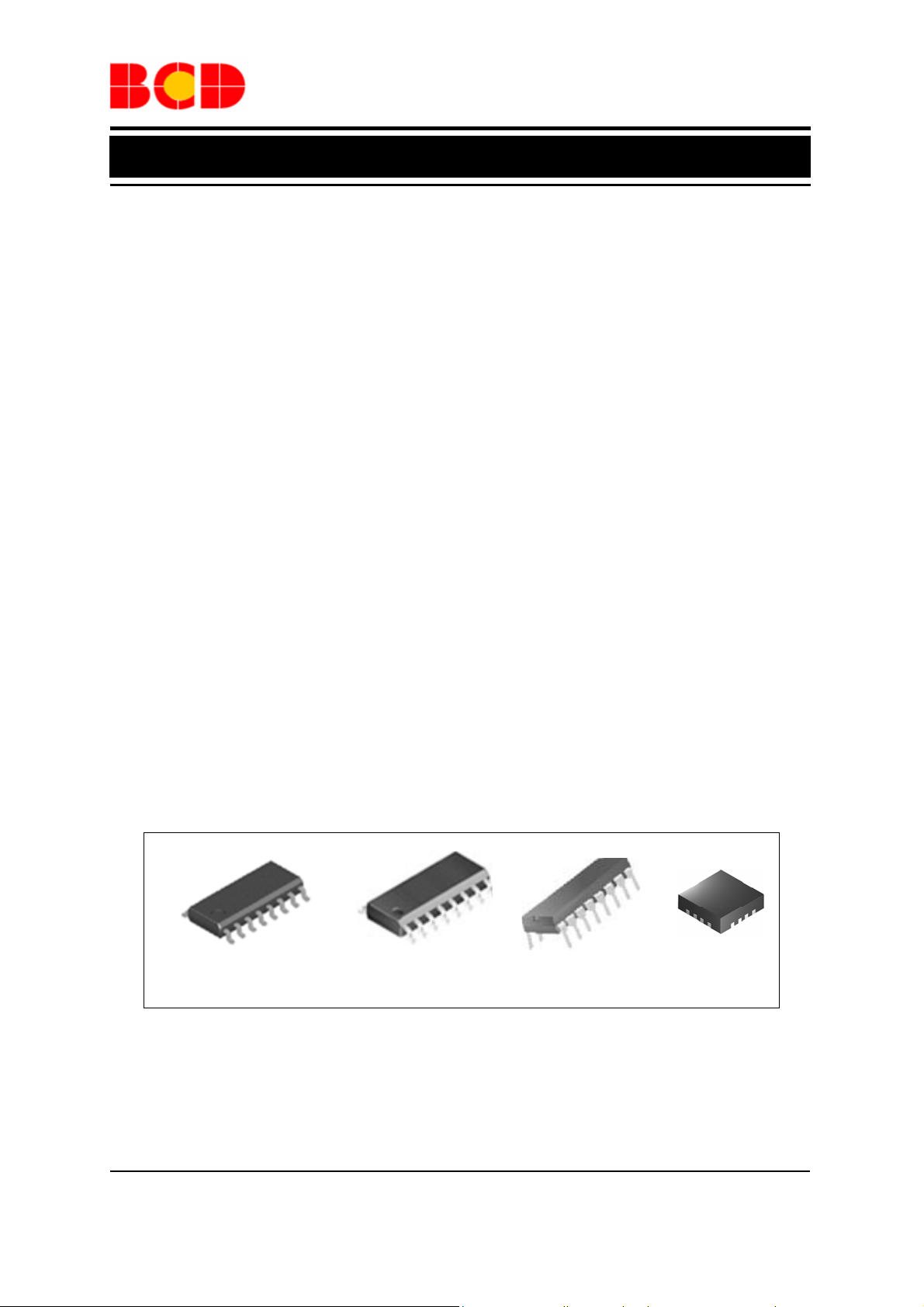
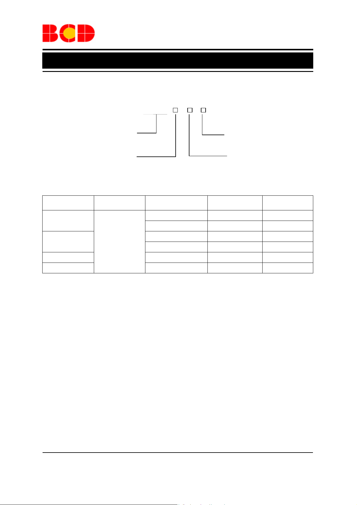
The AP3064 is available in SOIC-16, PSOP-16,
DIP-16 and QFN-4×4-16 package s.
OUT
Features
• Input Voltage Range: 4.5V to 33V
• Drives up to 4 Strings in Parallel, 220mA per
String
• Programmable WLED Current from 20mA to
220mA
• Adjustable Operating Frequency: 100kHz to
1MHz
• String-to-string Current Matching Accuracy:
1.5%
• Built-in OCP, OTP, UVLO
• External PWM Dimming
• Open/Short LED Protection
• Programmable Soft-start
• Programmable OVP
• Schottky Diode/Inductor Short-circuit Protection
• V
Short/Schottky Diode Open Protection
OUT
Applications
• LCD Monitor
• LCD Display Module
• LCD TV
SOIC-16 PSOP-16 DIP-16 QFN-4×4-16
Figure 1. Package Types of AP3064
Jul. 2012 Rev. 1. 5 BCD Semiconductor Manufacturing Limited
1
Page 2
Preliminary Datasheet
Boost Type LED Driver with 4-Channel Current Source AP3064
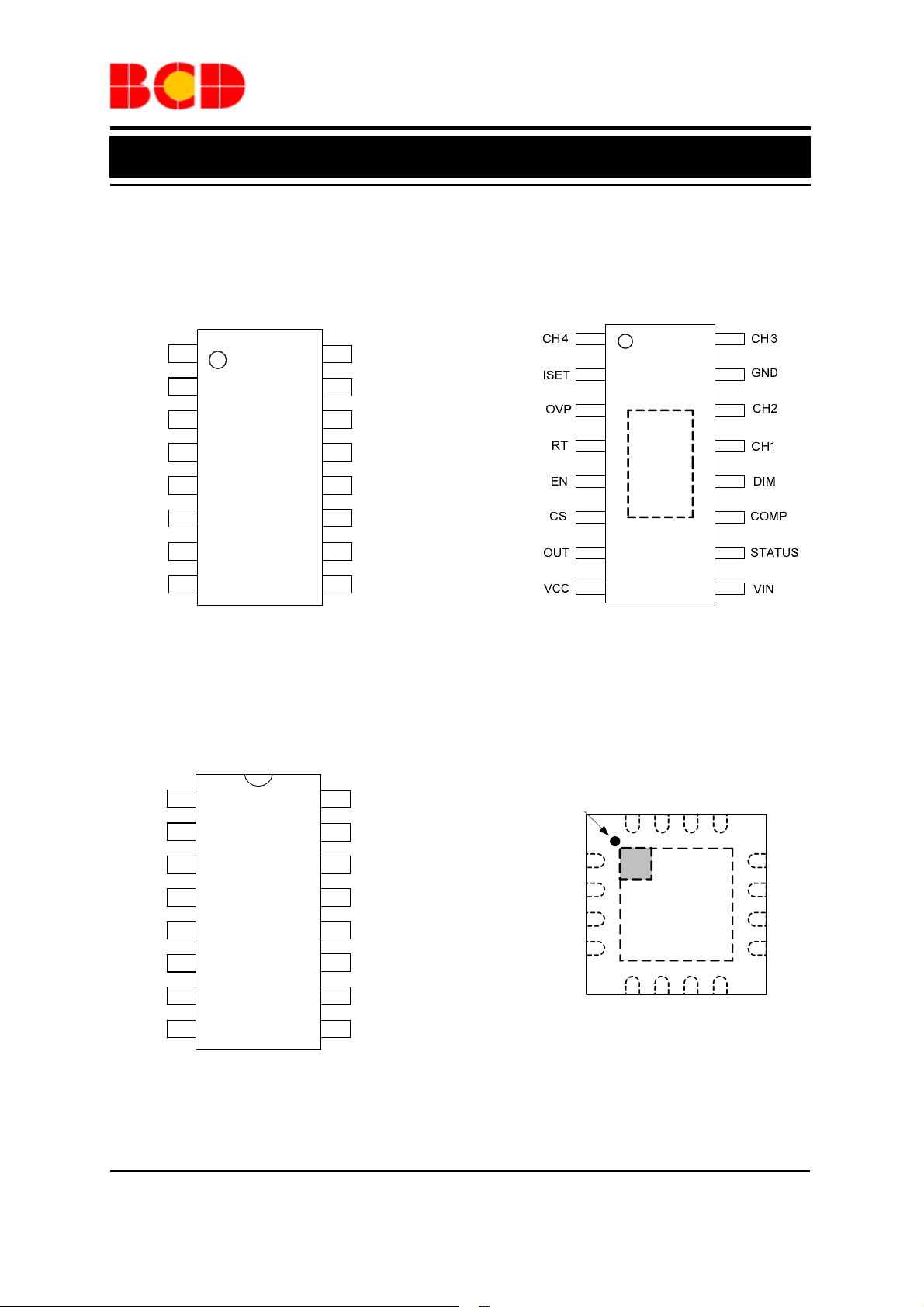
Pin Configuration
M Package MP Package
(SOIC-16) (PSOP-16)
1
CH4
2
ISET
OVP
3
4
RT
5
EN
CS
6
7
OUT
8
VCC VIN
P Package FN Package
(DIP-16) (QFN-4×4-16)
CH4
1
OVP
2
ISET
3
RT
4
EN
5
CS
6
OUT
7
VCC VIN
8
Figure 2. Pin Configuration of AP3064 (Top View)
16
15
14
13
12
11
10
9
CH3
GND
CH2
CH1
DIM
COMP
STATUS
1
2
3
4
5
6
7
89
16
15
14
13
12
11
10
CH3
16
15
GND
CH2
14
CH1
13
DIM
12
COMP
11
10
STATUS
9
Pin 1 Mark
GND
CH3
CH4
OVP
1
2
3
4
CH1
CH2
16 15 14
E P
RT
ISET
DIM
EN
COMP
13
12
STATUS
11
VIN
10
VCC
9
OUT
8765
CS
Jul. 2012 Rev. 1. 5 BCD Semiconductor Manufacturing Limited
2
Page 3
µ
Preliminary Datasheet
Boost Type LED Driver with 4-Channel Current Source AP3064
Pin Description
Pin Number
SOIC-16
/PSOP-16
1 1 3 CH4
2 3 5 ISET
3 2 4 OVP
4 4 6 RT Frequency control pin
5 5 7
6 6 8
7 7 9 OUT
8 8 10 VCC
9 9 11 VIN
10 10 12 STATUS LED operation status output
DIP-16
QFN-
4×4-16
Pin
Name
EN
CS
Function
LED current sink 4. Leave the pin open
directly if not used
LED current setting pin. The corresponding
maximum current of all 4 strings is set through
connecting a resistor from this pin to GND
Over voltage protection pin. When the OVP
pin voltage exceeds 2.0V, the OVP is triggered
and the power switch is turned off. When the
OVP pin voltage drops below hysteresis
voltage, the OVP is released and the power
switch will resume normal operation
ON/OFF control pin. Forcing this pin above
2.4V enables the IC while below 0.5V shuts
down the IC. When the IC is in shutdown
mode, all functions are disabled to decrease
the supply current below 3µA
Power switch current sense input
Boost converter power switch gate output.
This pin output high voltage (5V/VIN-0.5V) to
drive the external N-MOSFET
5V linear regulator output pin. This pin should
be bypassed to GND (recommend to connect
with GND pin) with a ceramic capacitor
Supply input pin. A capacitor (typical 10
should be connected between the V
GND to keep the DC input voltage constant
and
IN
F)
11 11 13 COMP Soft-start and control loop compensation
PWM dimming control pin.
12 12 14 DIM
13 13 15 CH1
14 14 16 CH2
15 15 1 GND Ground
16 16 2 CH3
Adding a PWM signal to this pin to control
LED dimming. If not used, connect it to the
high level
LED current sink 1. Leave the pin open
directly if not used
LED current sink 2. Leave the pin open
directly if not used
LED current sink 3. Leave the pin open
directly if not used
Jul. 2012 Rev. 1. 5 BCD Semiconductor Manufacturing Limited
3
Page 4
Preliminary Datasheet
Boost Type LED Driver with 4-Channel Current Source AP3064
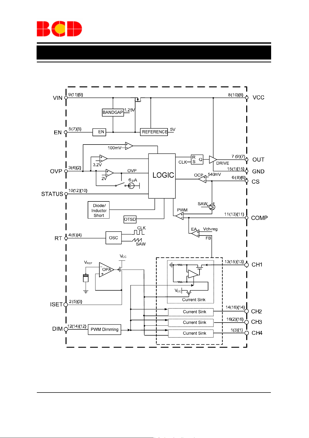
Functional Block Diagram
A(B){C}
A for SOIC-16 and PSOP-16
B for QFN-4×4-16
C for DIP-16
Figure 3. Function Block Diagram of AP3064
Jul. 2012 Rev. 1. 5 BCD Semiconductor Manufacturing Limited
4
Page 5
Preliminary Datasheet
Boost Type LED Driver with 4-Channel Current Source AP3064
Ordering Information
AP3064 -
G1: Green
Blank: Tube
TR: Tape & Reel
Package
SOIC-16
Circuit Type
Package
M: SOIC-16
MP: PSOP-16
P: DIP-16
FN: QFN-4×4-16
Temperature
Range
Part Number Marking ID Packing Type
AP3064M-G1 AP3064M-G1 Tube
AP3064MTR-G1 AP3064M-G1 Tape & Reel
PSOP-16
DIP-16 AP3064P-G1 AP3064P-G1 Tube
QFN-4×4-16 AP3064FNTR-G1 BJA Tape & Reel
-40 to 85°C
AP3064MP-G1 AP3064MP-G1 Tube
AP3064MPTR-G1 AP3064MP-G1 Tape & Reel
BCD Semiconductor's Pb-free products, as designated with "G1" suffix in the part number, are RoHS compliant
and green.
Jul. 2012 Rev. 1. 5 BCD Semiconductor Manufacturing Limited
5
Page 6
Preliminary Datasheet
Boost Type LED Driver with 4-Channel Current Source AP3064
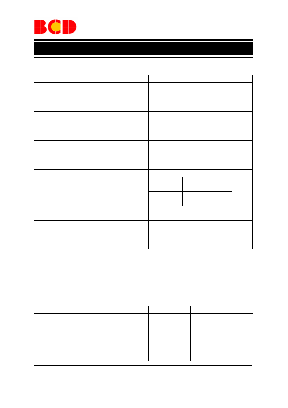
Absolute Maximum Ratings (Note 1)
Parameter Symbol Value Unit
Input Voltage
CH1 to CH4 Voltage
EN Pin Voltage
VCC Pin Voltage
CS Pin Voltage
COMP Pin Voltage
ISET Pin Voltage
OUT Pin Voltage
OVP Pin Voltage
RT Pin Voltage
STATUS Pin Voltage
DIM Pin Voltage
GND Pin Voltage
V
V
V
VCC
V
V
COMP
V
V
V
V
V
STATUS
V
V
IN
CH
EN
CS
ISET
OUT
OVP
RT
DIM
GND
SOIC-16 100
Thermal Resistance (Junction to
Ambient, Free Air, No Heatsink)
θ
JA
PSOP-16 50
DIP-16 85
QFN-4×4-16 55
Operating Junction Temperature
Storage Temperature
T
J
T
STG
Lead Temperature
T
(Soldering, 10sec)
LEAD
ESD (Machine Model) 200 V
ESD (Human Body Model) 2000 V
Note 1: Stresses greater than those listed under “Absolute Maximum Ratings” may cause permanent damage to
the device. These are stress ratings only, and functional operation of the device at these or any other conditions
beyond those indicated under “Recommended Operating Conditions” is not implied. Exposure to “Absolute
Maximum Ratings” for extended periods may affect device reliability.
Note 2: Negative CS 100ns Transient maximum rating voltage reach to -0.4V.
-0.3 to 42 V
-0.3 to 65 V
-0.3 to 7 V
-0.3 to 7 V
-0.3 to 7 V
-0.3 to 7 V
-0.3 to 7 V
-0.3 to 7 V
-0.3 to 7 V
-0.3 to 7 V
-0.3 to 7 V
-0.3 to 7 V
-0.3 to 0.3 V
ºC/W
150 ºC
-65 to 150 ºC
260 ºC
Recommended Operating Conditions
Parameter Symbol Min Max Unit
Input Voltage V
IN
Operating Frequency fO 0.1 1 MHz
LED Channel Voltage V
LED Channel Current I
PWM Dimming Frequency f
Operating Ambient Temperature
Range
Jul. 2012 Rev. 1. 5 BCD Semiconductor Manufacturing Limited
60 V
CHX
20 180 mA
CHX
0.1 20 kHz
PWM
-40 85 ºC
T
A
6
4.5 33 V
Page 7

Preliminary Datasheet
Boost Type LED Driver with 4-Channel Current Source AP3064
Electrical Characteristics
V
=24V, VEN=5V, Typical TA=25°C, unless otherwise specified.
IN
Parameter Symbol Conditions Min Typ Max Unit
INPUT SUPPLY
Input Voltage VIN 4.5 33 V
Quiescent Current IQ No Switching 3 5 mA
Shutdown Supply Current I
UVLO V
UVLO Hysteresis V
SHTD
UVLO
HYS
VCC SECTION
VCC Voltage VCC
OUT Pin Rising Time (Note 3) t
OUT Pin Falling Time (Note 3) t
RISING
FALLING
Load Regulation (Note 3)
Line Regulation (Note 3)
HIGH FREQUENCY OSCILLATOR
Switch Frequency
(Target: 10% Variation)
Switch Frequency
Range
Maximum Duty Cycle D
f
OSC
0.1 1 MHz
MAX
VEN=VDD=0V 0.1 3
V
Rising 3.6 3.8 4.0 V
IN
µA
200 mV
≥5.5V
V
IN
VIN<5.5V,
Load=10mA
5 V
V
-0.1 V
IN
1nF Load 30 50 ns
1nF Load 30 50 ns
Load=0 to
30mA
=5.5 to
V
IN
24V
=100kΩ
R
T
5
0.3
440 520 600 kHz
mV/mA
mV/V
f=500kHz 88 90 %
Minimum On-time (Note 3) t
f=500kHz 200 ns
ON-TIME
ENABLE LOGIC AND DIMMING LOGIC
EN High Voltage V
EN Low Voltage V
PWM Logic for External Dimming
PWM Dimming Minimum Pulse
Width (Note 3)
t
2.4 V
EN_H
0.5 V
EN_L
V
2.5 V
DIM_H
V
0.3 V
DIM_L
PWM_MIN
3/f
OSC
µs
Jul. 2012 Rev. 1. 5 BCD Semiconductor Manufacturing Limited
7
Page 8

Preliminary Datasheet
Boost Type LED Driver with 4-Channel Current Source AP3064
Electrical Characteristics (Continued)
V
=24V, VEN=5V, Typical TA=25°C, unless otherwise specified.
IN
Parameter Symbol Conditions Min Typ Max Unit
POWER SWITCH DRIVE
Current Limit Threshold Voltage V
D/L Short Threshold Voltage
(Note 3)
Current Sense LEB Time
(Note 3)
480 540 600 mV
LIMIT
V
720 800 880 mV
LIMIT2
80 100 150 ns
t
LEB
COMPENSATION AND SOFT START (COMP PIN)
Error Amplifier
Trans-conductance
Sourcing Current I
Sinking Current I
2300
G
EA
V
O_H
V
O_L
COMP
COMP
OVER-VOLTAGE PROTECTION
OVP Threshold Voltage V
OVP Hysteresis V
Shutdown Under Abnormal
Condition
OVP
OVP_HYS
V
OVP-SH
V
OUT
250 mV
3.0 3.2 3.4 V
CURRENT SOURCE
LED Current Matching between
Each String (Note 4)
I
CH_MATCHICH
Regulation Current per Channel ICH
Minimum LED Regulation
Voltage
CH1 to CH4 Leakage Current I
LED Short Protection Threshold V
V
LED_REGICHX
LED_LEAK
LED-S
6.6 7.3 8.0 V
=100mA
R
ISET
VEN=0V,
V
LED
OVER-TEMPERATURE PROTECTION
Thermal Shutdown Temperature
(Note 3)
Thermal Shutdown Recovery
(Note 3)
160 ºC
T
OTSD
140 ºC
T
HYS
Note 3: Guaranteed by design.
Note 4:
I
_
=
MATCHST
2
MINMAX
I
×
×
AVG
%100
II
−
µA/V
=0.5V 80 120 160
=2V 80 120 160
µA
µA
Rising 1.9 2.0 2.1 V
=12kΩ
92 100 108 mA
1.5 4 %
=100mA 230 mV
=37V
0.1 1
µA
Jul. 2012 Rev. 1. 5 BCD Semiconductor Manufacturing Limited
8
Page 9

Preliminary Datasheet
Boost Type LED Driver with 4-Channel Current Source AP3064
Typical Performance Characteristics
=24V, VEN=VDD=5V, 13 LEDs in series, 4 strings in parallel, 120mA/string, TA=25°C, unless otherwise
V
IN
specified.
1200
1100
1000
900
800
700
600
500
Frequency (kHz)
400
300
200
100
0
0 100 200 300 400 500 600 700
Figure 4. Frequency vs. R
RT (kΩ)
5.4
T
5.2
5.0
4.8
4.6
4.4
4.2
VCC Voltage(V)
4.0
3.8
3.6
4 6 8 10121416182022242628303234
C
=2.2µF
VCC
Input Voltage(V)
Figure 5. VCC Voltage vs. Input Voltage
0.60
0.55
0.50
0.45
0.40
0.35
0.30
0.25
Regulation Voltage (V)
CH
V
0.20
0.15
0.10
60 80 100 120 140 160 180 200 220
Output Current /CH (mA)
RT=100k
0.50
0.45
0.40
0.35
0.30
0.25
0.20
0.15
Regulation Voltage (V)
CH
V
0.10
0.05
0.00
-50 -25 0 25 50 75 100 125 150
Temperature (oC)
VIN=24V, R
ISET
=10k
Figure 6. VCH Regulation Voltage vs. Output Current Figure 7. V
Regulation Voltage vs. Temperature
LED
Jul. 2012 Rev. 1. 5 BCD Semiconductor Manufacturing Limited
9
Page 10

m
m
Preliminary Datasheet
Boost Type LED Driver with 4-Channel Current Source AP3064
Typical Performance Characteristics (Continued)
VIN=24V, VEN=VDD=5V, 13 LEDs in series, 4 strings in parallel, 120mA/string, TA=25°C, unless otherwise
specified.
240
220
200
180
160
140
120
100
80
60
Channel Current (mA)
40
20
0
012345
Channel
I
SET
I
SET
I
SET
I
SET
I
SET
=220mA
=180mA
=160mA
=120mA
=60mA
98
96
94
92
90
88
Efficiency (%)
86
84
82
80
0 100 200 300 400 500 600 700 800
Figure 8. Channel Current vs. Channel Figure 9. Efficiency vs. Output Current
VIN=24V
LED: 4P13S
Output Current (mA)
V
SW
50V/div
ICH
20mA/div
V
OUT_AC
500
V/div
V
200
CH
V/div
100mA/div
20V/div
20V/div
20V/div
V
V
V
OUT
I
IN
SW
CH
Time 1µs/div
Time 20ms/div
Figure 10. Steady State Figure 11. System Startup
Jul. 2012 Rev. 1. 5 BCD Semiconductor Manufacturing Limited
10
Page 11

m
Preliminary Datasheet
Boost Type LED Driver with 4-Channel Current Source AP3064
Typical Performance Characteristics (Continued)
VIN=24V, VEN=VDD=5V, 13 LEDs in series, 4 strings in parallel, 120mA/string, TA=25°C, unless otherwise
specified.
V
PWM
5V/div
VSW
20V/div
V
STATUS
5V/div
V
50V/div
I
100mA/div
CH
SW
ICH
100
A/div
V
CH
5V/div
Time 2ms/div
Time 10µs/div
Figure 12. PWM Dimming Figure 13. LED Short Protection
V
STATUS
5V/div
50V/div
50mA/div
V
ICH
SW
V
SW
50V/div
V
STATUS
5V/div
V
1V/div
CS
V
OVP
1V/div
I
CH
50mA/div
Time 50ms/div
Time 50µs/div
Figure 14. LED Open Protection Figure 15. Schottky/Inductor Short Protection
Jul. 2012 Rev. 1. 5 BCD Semiconductor Manufacturing Limited
11
Page 12

Preliminary Datasheet
Boost Type LED Driver with 4-Channel Current Source AP3064
Typical Performance Characteristics (Continued)
VIN=24V, VEN=VDD=5V, 13 LEDs in series, 4 strings in parallel, 120mA/string, TA=25°C, unless otherwise
specified.
V
V
10V/div
V
OVP
5V/div
V
GATE
5V/div
I
CH
50mA/div
IN
Figure 16. V
Time 5ms/div
Short/Diode Open Protection Figure 17. Over Temperature Protection
OUT
SW
50V/div
V
STATUS
5V/div
V
OUT
50V/div
I
CH
50mA/div
Time 1s/div
Jul. 2012 Rev. 1. 5 BCD Semiconductor Manufacturing Limited
12
Page 13

+
Preliminary Datasheet
Boost Type LED Driver with 4-Channel Current Source AP3064
Application Information
1. Enable
The AP3064 is enable when the voltage to EN is greater
than approximately 2.4V, disabled when lower than
0.5V.
2. Frequency Selection
An external resistor RT, placed between RT pin and
GND, can be used to set the operating frequency. The
operating frequency ranges from 100kHz to 1MHz.
The high frequency operation optimizes the r egulator
for the smallest-sized component application, while
low frequency operation can help to reduce switch
loss. The approximate operating frequency can be
expressed as below:
OSC
][
MHzf
52
=
RT
][
Ω
KR
3. LED Current Setting
The maximum LED current per channel can be
adjusted up to 180mA via ISET pin. When ≥180mA
current is needed in application, two or more
channels can be paralleled to provide larger drive
current. Connect a resistor R
and GND to set the reference current I
current can be expressed as below:
1200
][
=
mAI
LED
ISET
][
Ω
KR
between ISET pin
ISET
SET
. The LED
4. Dimming Control
Applying a PWM signal to DIM pin to adjust the
LED current, that means, the LED current of all
enabled channels can be adjusted at the same time
and the LED brightness can be adjusted from 1%×
I
CHX_MAX
level” period of PWM signal, the LED is turned on
and 100% of the current flows through LED, while
during the “low level” period of the PWM signal, the
LED is turned off and almost no current flows
through the LED, thus cha nging the average current
through LED and finally adjusting LED brightness.
The external PWM signal frequency applied to PWM
pin is allowed to be 100Hz or higher.
to 100%× I
CHX_MAX
. During the “high
5. Status Output
After IC is enabled, STATUS will output logic low if
any of the following conditions exists:
(1) Any String is Open
(2) LED Short Circuit Protection
(3) Shut Down Under Abnormal Condition
(4) Over Voltage Protection
(5) Over Temperature Protection
(6) Schottky Diode Short Protection
(7) V
Short/Open Schottky Diode Protection
OUT
6. Over Voltage Protection
The AP3064 integrates an OVP circuit. The OVP pin
is connected to the center tap of voltage-divider (R
and R
and GND. If the voltage on OVP pin exceeds 2.0V,
which may results from open loop or excessive
output voltage, all the functions of AP3064 will be
disabled with output voltage falling. The OVP
hysteresis is 250mV. The formulas of OVP can be
expressed as below:
V
) that placed between high voltage output
OV2
2.0V)R(R
×
=
OVP
OV2OV1
R
OV2
7. Over Current Protection
The AP3064 integrates an OCP circuit. The CS pin is
connected to the voltage-sensor (R
between the Drain of MOS and GND. If the voltage
on CS pin exceeds 0.54V, it is turned off immediately
and will not turn on until the next cycle begins.
) that placed
CS
8. LED Short-Circuit Protection
The AP3064 integrates an LED Short-circuit
protection circuit. If the voltage at any of the CH1-4
pins exceeds a threshold of approximately 7.3V
during normal operation, the corresponding str ing is
turned off and is latched off. Toggle V
reset the latch. LED short detecting logic priority is
lower than open LED and OVP logic. The LED short
detecting is triggered when 0.1V<V
dimming on mode, disabled when LED open occurs
until output voltage resumes to the regulated voltage.
and/or EN to
IN
LED_MIN
under
OV1
Jul. 2012 Rev. 1. 5 BCD Semiconductor Manufacturing Limited
13
Page 14

Preliminary Datasheet
Boost Type LED Driver with 4-Channel Current Source AP3064
Application Information (Continued)
9. LED Open-circuit Protection
The AP3064 integrates an LED Open-circuit
Protection circuit. When any LED string is open,
V
will boost up until the voltage at OVP pin
OUT
reaches an approximate 2.0V threshold. The IC will
automatically ignore the open string whose
corresponding pin voltage is less than 100mV and the
remaining string will continue operation. If all the
strings are open and the voltage at OVP reaches a
threshold of 2.0V, the MOSFET drive GATE will turn
off and IC will shut down and latch.
10. V
Short / Open Schottky Diode
OUT
Protection
The AP3064 monitors the OVP pin, if the OVP pin
voltage is less than 0.1V, MOSFET drive output will
turn off. This protects the converter if the output
Schottky diode is open or V
is shorted to ground.
OUT
11. Under Voltage Lockout
The AP3064 provides an under voltage lockout
circuit to prevent it from undefined status when
startup. The UVLO circuit shuts down the device
when V
200mV hysteresis, which means the device starts up
again when V
drops below 3.6V. The UVLO circuit has
CC
rise to 3.8V.
CC
12. Over Temperature Protection
The AP3064 features Over Temperature Protection, if
the junction temperature exceeds approximately
160ºC, the IC will shut down until the junction
temperature is less than approximately 140ºC. When
the IC is released from over temperature shutdown, it
will start a soft-start process.
13. Schottky Diode/Inductor Short Circuit Protection
The AP3064 features Schottky diode/inductor
short-circuit protection circuit. When CS pin voltage
exceeds 0.8V for greater than 16 switching clocks,
the IC will latch. The voltage of CS is monitored
after a short delay of LEB.
14. Shut Down under Abnormal Condition
The AP3064 features shutdown under abnormal
condition protection circuit. When OVP pin voltage
exceeds 3.2V, the IC will latch. Toggle EN to restart
the IC. This feature can be used for any other
protection to shut down the IC.
Jul. 2012 Rev. 1. 5 BCD Semiconductor Manufacturing Limited
14
Page 15

Preliminary Datasheet
Boost Type LED Driver with 4-Channel Current Source AP3064
Typical Application
V
IN
C
1
22
F
R
0
4
C
5
NC
ON OFF
R
300k
R
10k
6
5
EN
RT
R
120k
STATUS
ON OFF
T
0.22
R15
1k
C
R14
7
F
100k
R8
R7
300k
10k
C
2.2
VCC
COMP
VCC
F
STATUS
DIM
L
OUTVIN
CS
OVP
CH1
---
CH4
ISET
GND
47 H
R
NC
600 @100MHz
2
13
R
0
3
C
2
R
ISET
10k
0.3
Q1
FB
D1
C
22 F
R
R
1
0.3
2
3
C
820pF
C
4
22 F
R
1M
R
36k
OV1
OV2
V
OUT
13X4
Figure 18. Typical Application Circuit of AP3064
Jul. 2012 Rev. 1. 5 BCD Semiconductor Manufacturing Limited
15
Page 16

Preliminary Datasheet
Boost Type LED Driver with 4-Channel Current Source AP3064
Mechanical Dimensions
SOIC-16 Unit: mm(inch)
1.350(0.053)
1.750(0.069)
0.330(0.013)
0.510(0.020)
B
7
°
1.250(0.049)
1.650(0.065)
5
2
.
0
(
0
7
°
0
.
0
A
20:1
)
0
1
0.400(0.016)
1.270(0.050)
3°
7°
8
°
5.800(0.228)
6.240(0.246)
3.800(0.150)
4.040(0.159)
9
.
5
°
8
°
0.400(0.016)×45°
8°
0°
8°
R0.200(0.008)
R0.200(0.008)
.
0
.
0
(
0
5
0
.
0
0
5
2
.
0
B
20:1
C
φ
S 1.000(0.039)
Depth 0.200(0.008)
A
C
)
2
0
0
0
.
0
(
)
0
1
0.200(0.008)
0
C-C
50:1
2
2
.
0
0
.
0
(
0
0
0
5
)
8
0
(
)
0
1
0
.
Note: Eject hole, oriented hole and mold mark is optional.
Jul. 2012 Rev. 1. 5 BCD Semiconductor Manufacturing Limited
16
Page 17

Preliminary Datasheet
Boost Type LED Driver with 4-Channel Current Source AP3064
Mechanical Dimensions (Continued)
PSOP-16 Unit: mm(inch)
Jul. 2012 Rev. 1. 5 BCD Semiconductor Manufacturing Limited
17
Page 18

Preliminary Datasheet
Boost Type LED Driver with 4-Channel Current Source AP3064
Mechanical Dimensions (Continued)
DIP-16 Unit: mm(inch)
0.700(0.028)
3.200(0.126)
3.600(0.142)
6°
4°
1.524(0.060) TYP
3.710(0.146)
4.310(0.170)
7.320(0.288)
7.920(0.312)
5°
6°
4°
0.360(0.014)
0.560(0.022)
R0.750(0.030)
Note: Eject hole, oriented hole and mold mark is opt ional.
2.540(0.100)
TYP
18.800(0.740)
19.200(0.756)
0.510(0.020)MIN
3.000(0.118)
3.600(0.142)
6.200(0.244)
6.600(0.260)
0.204(0.008)
0.360(0.014)
8.200(0.323)
9.400(0.370)
Φ3.000(0.118)
Depth
0.050(0.002)
0.150(0.006)
Jul. 2012 Rev. 1. 5 BCD Semiconductor Manufacturing Limited
18
Page 19

Preliminary Datasheet
Boost Type LED Driver with 4-Channel Current Source AP3064
Mechanical Dimensions (Continued)
QFN-4×4-16 Unit: mm(inch)
Jul. 2012 Rev. 1. 5 BCD Semiconductor Manufacturing Limited
19
Page 20

BCD Semiconductor Manufacturing Limited
IMPORTANT NOTICE
IMPORTANT NOTICE
BCD Semiconductor Manufacturing Limited reserves the right to make changes without further notice to any products or specifi-
BCD Semiconductor Manufacturing Limited reserves the right to make changes without further notice to any products or specifi-
cations herein. BCD Semiconductor Manufacturing Limited does not assume any responsibility for use of any its products for any
cations herein. BCD Semiconductor Manufacturing Limited does not assume any responsibility for use of any its products for any
particular purpose, nor does BCD Semiconductor Manufacturing Limited assume any liability arising out of the application or use
particular purpose, nor does BCD Semiconductor Manufacturing Limited assume any liability arising out of the application or use
of any its products or circuits. BCD Semiconductor Manufacturing Limited does not convey any license under its patent rights or
of any its products or circuits. BCD Semiconductor Manufacturing Limited does not convey any license under its patent rights or
other rights nor the rights of others.
other rights nor the rights of others.
http://www.bcdsemi.com
MAIN SITE
MAIN SITE
- Headquarters
BCD Semiconductor Manufacturing Limited
BCD Semiconductor Manufactur ing Limited
- Wafer Fab
No. 1600, Zi Xing Road, Shanghai ZiZhu Science-based Industrial Park, 200241, China
Shanghai SIM-BCD Semiconductor Manufacturing Limited
Tel: +86-21-24162266, Fax: +86-21-24162277
800, Yi Shan Road, Shanghai 200233, China
Tel: +86-21-6485 1491, Fax: +86-21-5450 0008
REGIONAL SALES OFFICE
Shenzhen Office
REGIONAL SALES OFFICE
Shanghai SIM-BCD Semiconductor Manufacturing Co., Ltd., Shenzhen Office
Shenzhen Office
Unit A Room 1203, Skyworth Bldg., Gaoxin Ave.1.S., Nanshan District, Shenzhen,
Shanghai SIM-BCD Semiconductor Manufacturing Co., Ltd. Shenzhen Office
China
Advanced Analog Circuits (Shanghai) Corporation Shenzhen Office
Tel: +86-755-8826 7951
Room E, 5F, Noble Center, No.1006, 3rd Fuzhong Road, Futian District, Shenzhen 518026, China
Fax: +86-755-8826 7865
Tel: +86-755-8826 7951
Fax: +86-755-8826 7865
- Wafer Fab
BCD Semiconductor Manufacturing Limited
Shanghai SIM-BCD Semiconductor Manufacturing Co., Ltd.
- IC Design Group
800 Yi Shan Road, Shanghai 200233, China
Advanced Analog Circuits (Shanghai) Corporation
Tel: +86-21-6485 1491, Fax: +86-21-5450 0008
8F, Zone B, 900, Yi Shan Road, Shanghai 200233, China
Tel: +86-21-6495 9539, Fax: +86-21-6485 9673
Taiwan Office
BCD Semiconductor (Taiwan) Company Limited
Taiwan Office
4F, 298-1, Rui Guang Road, Nei-Hu District, Taipei,
BCD Semiconductor (Taiwan) Company Limited
Tai wan
4F, 298-1, Rui Guang Road, Nei-Hu District, Taipei,
Tel: +886-2-2656 2808
Taiwan
Fax: +886-2-2656 2806
Tel: +886-2-2656 2808
Fax: +886-2-2656 2806
USA Office
BCD Semiconductor Corp.
USA Office
30920 Huntwood Ave. Hayward,
BCD Semiconductor Corporation
CA 94544, USA
30920 Huntwood Ave. Hayward,
Tel : +1-510-324-2988
CA 94544, U.S.A
Fax: +1-510-324-2788
Tel : +1-510-324-2988
Fax: +1-510-324-2788
 Loading...