

Page 1

AP3036B
Document number: DS37004 Rev. 1 - 2
1 of 11
www.diodes.com
March 2014
© Diodes Incorporated
AP3036B
A Product Line of
Diodes Incorporated
NE W P R OD U C T
Description
The AP3036B is an inductor-based DC/DC converter designed to
drive up to eight white LEDs in series for backlight. Only one
feedback resistor is needed to control the LED current and obtain
required brightness.
A constant frequency 1.0MHz PWM control scheme is employed in
this IC, which means tiny external components can be used.
Specifically, 1mm tall inductor and 0.22µF output capacitor for a
typical application is sufficient. Additionally, the Schottky diode in
boost circuit is integrated on this chip. The AP3036B also provides a
disable pin to ease its use for different systems.
The output over-voltage protection is implemented in AP3036B. When
any LED is broken or in other abnormal conditions, the output voltage
will be clamped.
The AP3036B is available in standard SOT26 package.
Applications
Cellular Phones
Digital Cameras
LCD Modules
GPS Receivers
PDAs, Handheld Computers
Pin Assignments
(Top View)
SW
GND
FBCTRL
VOUT
VIN
1
2
3 4
5
Pin 1 Mark
6
SOT26
Features
Inherently Uniform LED Current
High Efficiency up to 84%
No Need for External Schottky Diode
Output Over-voltage Protection (OVP)
Fixed 1.0MHz Switching Frequency
Uses Tiny 1mm Tall Inductor
Requires Only 0.22µF Output Capacitor
High Frequency Dimming Control
Totally Lead-Free & Fully RoHS Compliant (Notes 1 & 2)
Halogen and Antimony Free. “Green” Device (Note 3)
22
1F
0.22F
10
VIN
SW VOUT
FB
GND
CTRL
AP3036B
Control
Signal
L
C
IN
C
OUT
V
IN
3V
WHITE LED STEP-UP CONVERTER
Notes: 1. No purposely added lead. Fully EU Directive 2002/95/EC (RoHS) & 2011/65/EU (RoHS 2) compliant.
2. See http://www.diodes.com/quality/lead_free.html for more information about Diodes Incorporated’s definitions of Halogen- and Antimony-free, "Green"
and Lead-free.
3. Halogen- and Antimony-free "Green” products are defined as those which contain <900ppm bromine, <900ppm chlorine (<1500ppm total Br + Cl) and
<1000ppm antimony compounds.
Typical Applications Circuit (Note 4)
Note 4: C: X5R or X7R type dielectric, L: SUMIDA CDRH5D28R-220NC or equivalent. And, this circuit can work in full temperature.
Page 2

AP3036B
Document number: DS37004 Rev. 1 - 2
2 of 11
www.diodes.com
March 2014
© Diodes Incorporated
AP3036B
A Product Line of
Diodes Incorporated
NE W P R OD U C T
Pin Number
Pin Name
Function
1
CTRL
Shutdown and dimming pin. Connect to 1.5V or higher to enable device; Connect to 0.4V or less to
disable device; Connect to a PWM signal to achieve LEDs brightness dimming
2
VOUT
Output pin. Connect to the cathode of internal Schottky diode
3
VIN
Input supply pin. Must be connected to a local bypass capacitor
4
SW
Switch pin. Connect external inductor
5
GND
Ground 6 FB
Voltage feedback pin. The reference voltage is 200mV
Q1
A2
A1
R
S
Q
1.0MHz
OSCILLATOR
RAMP
GENERATOR
V
REF
6
3
1
5
2
DRIVER
1.25V
COMPARATOR
OVP
200 mV
4
SOFT
START
FB SW
VOUT
GND
CTRL
VIN
Pin Descriptions
Functional Block Diagram
Page 3

AP3036B
Document number: DS37004 Rev. 1 - 2
3 of 11
www.diodes.com
March 2014
© Diodes Incorporated
AP3036B
A Product Line of
Diodes Incorporated
NE W P R OD U C T
Symbol
Parameter
Rating
Unit
VIN
Input Voltage
20
V
VSW
SW Pin Voltage
38
V
VFB
Feedback Voltage
20
V
V
CTRL
CTRL Pin Voltage
20
V
θ
JA
Thermal Resistance (Junction to Ambient, No Heat Sink)
265
C/W
TJ
Operating Junction Temperature
+150
C
T
STG
Storage Temperature Range
-65 to +150
C
T
LEAD
Lead Temperature (Soldering, 10sec)
+260
C
–
ESD (Machine Model)
250
V
–
ESD (Human Body Model)
2000
V
Symbol
Parameter
Min
Max
Unit
TOP
Operating Temperature Range
-40
+85
C
VIN
Input Voltage
2.5
16
V
V
CTRL
CTRL Pin Voltage
–
16
V
Absolute Maximum Ratings (Note 5)
Note 5: Stresses greater than those listed under "Absolute Maximum Ratings" may cause permanent damage to the device. These are stress ratings only, and
functional operation of the device at these or any other conditions beyond those indicated under "Recommended Operating Conditions" is not implied.
Exposure to "Absolute Maximum Ratings" for extended periods may affect device reliability.
Recommended Operating Conditions
Page 4

AP3036B
Document number: DS37004 Rev. 1 - 2
4 of 11
www.diodes.com
March 2014
© Diodes Incorporated
AP3036B
A Product Line of
Diodes Incorporated
NE W P R OD U C T
Symbol
Parameter
Conditions
Min
Typ
Max
Unit
VIN (Min)
Minimum Operating Voltage
–
2.5 – –
V
VIN (Max)
Maximum Operating Voltage
–
– – 16
VFB
Feedback Voltage
I
OUT
= 20mA, 4 LEDs
188
200
212
mV
IFB
FB Pin Bias Current
– – 35
100
nA
IQ
Quiescent Current
V
FB
= VIN, No Switching
1.6
3.1
3.9
mA
I
SHDN
Shutdown Quiescent Current
V
CTRL
= 0V
–
45
75
µA
f
Switching Frequency
– – 1.0 – MHz
D
MAX
Maximum Duty Cycle
–
90
93 – %
I
LIMIT
Switch Current Limit (Note 6)
D = 40% or 80%
–
550 – mA
V
CESAT
Switch VCE Saturation Voltage
I
SW
= 250mA
–
360 – mV
–
Switch Leakage Current
V
SW
= 5V
–
0.01 5 µA
V
CTRL
CTRL Pin Voltage
High
1.5
–
–
V
Low
– – 0.4
I
CTRL
CTRL Pin Bias Current
– – 100 – µA
VOV
OVP Voltage
– – 30 – V
V
DROP
Schottky Forward Drop
ID = 150mA
–
0.7 – V
–
Schottky Leakage Current
VR (Reverse Voltage) = 23V
–
0.1
4
µA
VR (Reverse Voltage) = 27V
– – 150
t
Soft Start Time
–
–
100 – µs
θ
JC
Thermal Resistance
(Junction to Case)
SOT26 – 60
–
C/W
Electrical Characteristics (@V
= 3V, V
IN
CTRL
= 3V, T
= +25°C, unless otherwise specified.)
A
Note 6: The switch current limit is related to duty cycle. Please refer to Figure LED Current vs. Duty (PWM Frequency = 0.5kHz).
Page 5
AP3036B
Document number: DS37004 Rev. 1 - 2
5 of 11
www.diodes.com
March 2014
© Diodes Incorporated
AP3036B
A Product Line of
Diodes Incorporated
NE W P R OD U C T
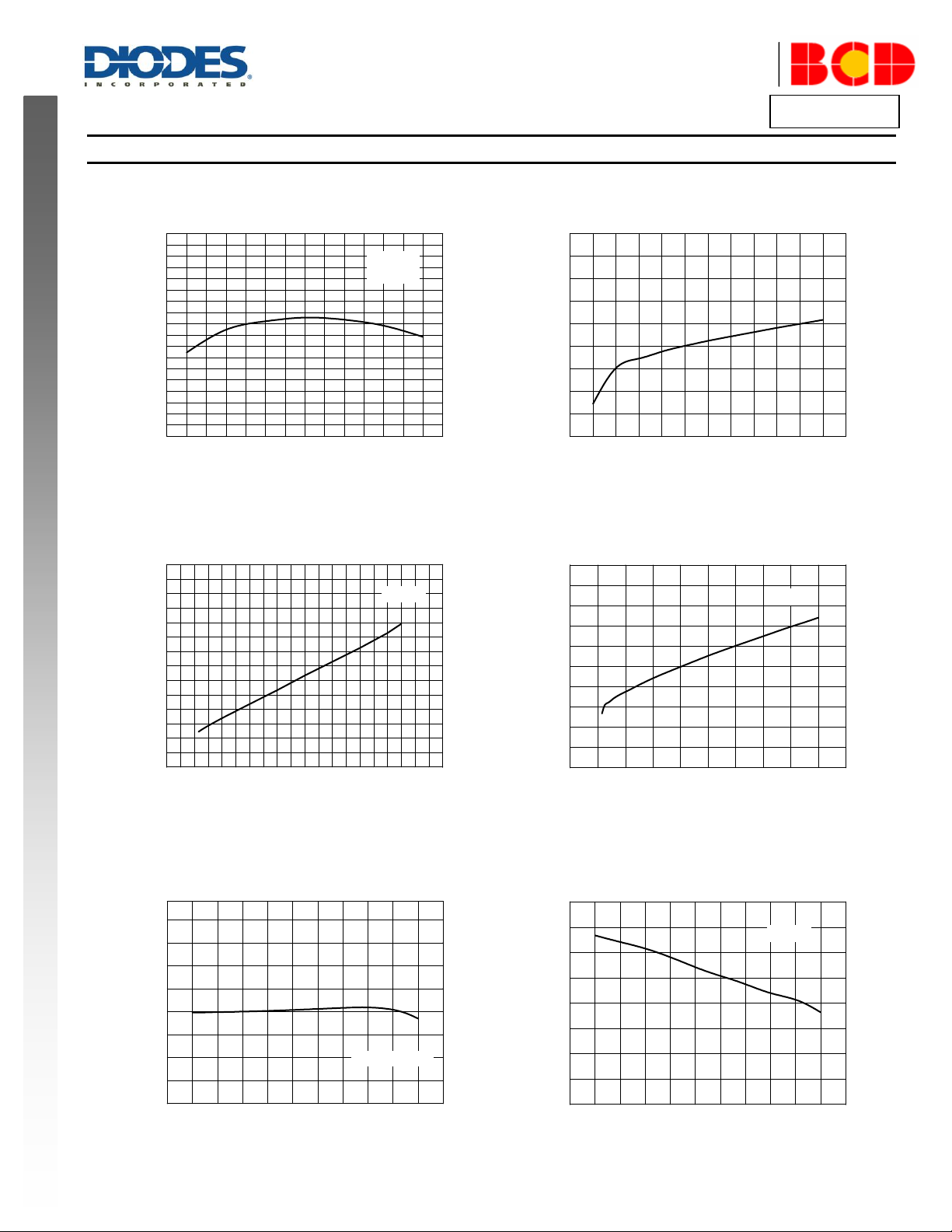
2 3 4 5 6 7 8
72
74
76
78
80
82
84
86
88
90
Efficiency (%)
LED Numbers
VIN=3.6V
I
OUT
=20mA
0 100 200 300 400 500
0
400
800
1200
1600
Schottky Forward Voltage (mV)
Schottky Forward Current (mA)
0 2 4 6 8 10 12 14 16 18 20
30
40
50
60
70
80
90
100
Shutdown Current (
A)
Input Voltage (V)
V
CTRL
=0V
0 4 8 12 16 20
2.8
3.0
3.2
3.4
3.6
3.8
Quiescent Current (mA)
Input Voltage (V)
VFB=1.0V
-40 0 40 80 120 160
100
150
200
250
300
Feedback Voltage (mV)
Temperature (OC)
VIN=3.6V, 5 LEDs
-40 0 40 80 120 160
300
400
500
600
Current Limit (mA)
Temperature (OC)
VIN=3.6V
Performance Characteristics (The WLED forward voltage (V
Efficiency vs. LED’s Number Schottky Forward Voltage vs.
Shutdown Current vs. Input Voltage Quiescent Current vs. Input Voltage
Feedback Voltage vs. Temperature Current Limit vs. Temperature
) is 3.45V at IF = 20mA, unless otherwise noted.)
F
Schottky Forward Current
Page 6
AP3036B
Document number: DS37004 Rev. 1 - 2
6 of 11
www.diodes.com
March 2014
© Diodes Incorporated
AP3036B
A Product Line of
Diodes Incorporated
NE W P R OD U C T
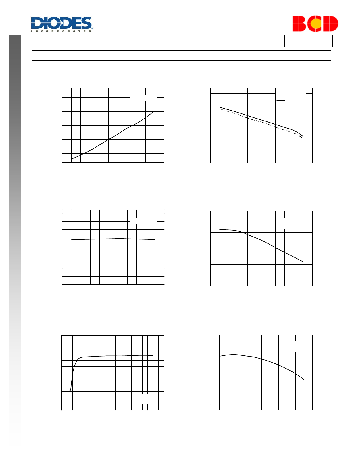
0 100 200 300 400 500
0
100
200
300
400
500
600
700
800
Saturation Voltage (mV)
Switch Current (mA)
VIN=V
CTRL
=3.6V
-40 0 40 80 120 160
0.0
0.4
0.8
1.2
CTRL Voltage (V)
Temperature (OC)
VIN=3.6V, 5 LEDs
Rising
Down
-40 0 40 80 120 160
20
24
28
32
36
OVP Voltage (V)
Temperature (OC)
VIN=V
CTRL
=3.6V
-40 0 40 80 120 160
0.6
0.8
1.0
1.2
Operating Frequency (MHz)
Temperature (OC)
VIN=3.6V
5 LEDs
2 4 6 8 10 12 14 16 18 20
60
65
70
75
80
85
90
Efficiency (%)
Input Voltage (V)
I
LED
=20mA
8 LEDs
20 30 40 50 60 70
60
64
68
72
76
80
84
88
Efficiency (%)
Output Current (mA)
VIN=3.6V
5 LEDs
Performance Characteristics (Cont. The WLED forward voltage (V
Saturation Voltage vs. Switch Current CTRL Pin Voltage vs. Temperature
) is 3.45V at IF = 20mA, unless otherwise noted.)
F
OVP Voltage vs. Temperature Operating Frequency vs. Temperature
Efficiency vs. Input Voltage Efficiency vs. Output Current
Page 7
AP3036B
Document number: DS37004 Rev. 1 - 2
7 of 11
www.diodes.com
March 2014
© Diodes Incorporated
AP3036B
A Product Line of
Diodes Incorporated
NE W P R OD U C T
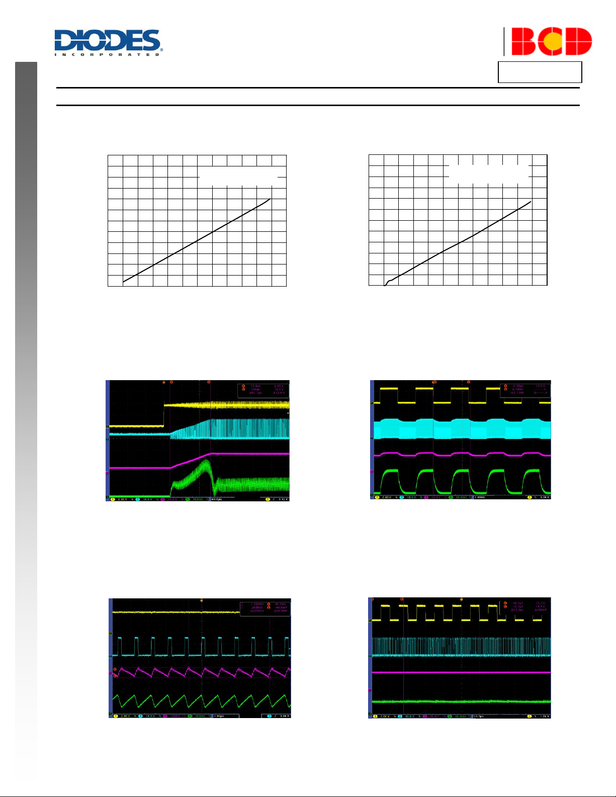
0 20 40 60 80 100
0
5
10
15
20
25
30
LED Current (mA)
Duty (%)
VIN=3.6V, 5 LEDs
PWM Frequency=0.5kHz
0 20 40 60 80 100
0
5
10
15
20
25
30
LED Current (mA)
Duty (%)
VIN=3.6V, 5 LEDs
PWM Frequency=100kHz
VIN
2V/div
VSW
10V/div
V
OUT
10V/div
IL
100mA/div
V
CTRL
2V/div
VSW
10V/div
V
OUT
I
LED
10mA/div
VIN
2V/div
VSW
10V/div
V
OUT1
(AC)
100mV/div
IL
100mA/div
VIN
2V/div
VSW
10V/div
V
OUT
10V/div
I
LED
10mA/div
Performance Characteristics (Cont. The WLED forward voltage (V
LED Current vs. Duty LED Current vs. Duty
Powering On PWM Dimming
(V
= 3.6V, V
IN
CTRL
= 2.5V, I
= 20mA, 5 LEDs) (V
LED
) is 3.45V at IF = 20mA, unless otherwise noted.)
F
= 3.6V, V
IN
PWM
= 2.5V, f
= 0.5kHz,
PWM
Duty = 50%, 5 LEDs)
Time 40s/div Time 10ms/div
(V
Output Voltage Ripple PWM Dimming
= V
IN
CTRL
= 3.6V, I
Time 1s/div Time 10s/div
= 20mA, 5 LEDs) (V
LED
= 3.6V, V
IN
PWM
= 2.5V, f
= 100kHz,
PWM
Duty = 50%, 5 LEDs)
Page 8
AP3036B
Document number: DS37004 Rev. 1 - 2
8 of 11
www.diodes.com
March 2014
© Diodes Incorporated
AP3036B
A Product Line of
Diodes Incorporated
NE W P R OD U C T
AP3036B X XX - XX
PackingPackageProduct Name
TR : Tape & Reel
K : SOT26
G1 : Green
RoHS/Green
Package
Temperature
Range
Part Number
Marking ID
Packing
SOT26
-40ºC to +85ºC
AP3036BKTR-G1
GHR
3000/7”Tape & Reel
XXX
: Logo
XXX: Marking ID (See Ordering Information)
Ordering Information
Diodes IC’s Pb-free products with "G1" suffix in the part number, are RoHS compliant and green.
Marking Information
(Top View)
Page 9
AP3036B
Document number: DS37004 Rev. 1 - 2
9 of 11
www.diodes.com
March 2014
© Diodes Incorporated
AP3036B
A Product Line of
Diodes Incorporated
NE W P R OD U C T
2.820(0.111)
3.100(0.122)
2.650(0.104)
3.000(0.118)
1.500(0.059)
1.700(0.067)
0.950(0.037)TYP
1.800(0.071)
2.000(0.079)
0.300(0.012)
0.500(0.020)
0.700(0.028)REF
0.100(0.004)
0.200(0.008)
0°
8°
0.200(0.008)
0.300(0.012)
0.600(0.024)
0.000(0.000)
0.150(0.006)
0.900(0.035)
1.300(0.051)
1.450(0.057)
MAX
1 2 3
4
5
6
Pin 1 Mark
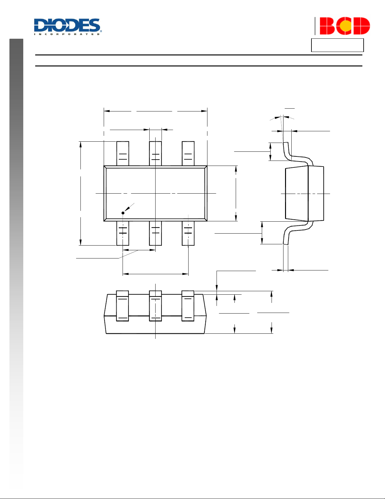
Package Outline Dimensions (All dimensions in mm(inch).)
(1) Package Type: SOT26
Page 10
AP3036B
Document number: DS37004 Rev. 1 - 2
10 of 11
www.diodes.com
March 2014
© Diodes Incorporated
AP3036B
A Product Line of
Diodes Incorporated
NE W P R OD U C T
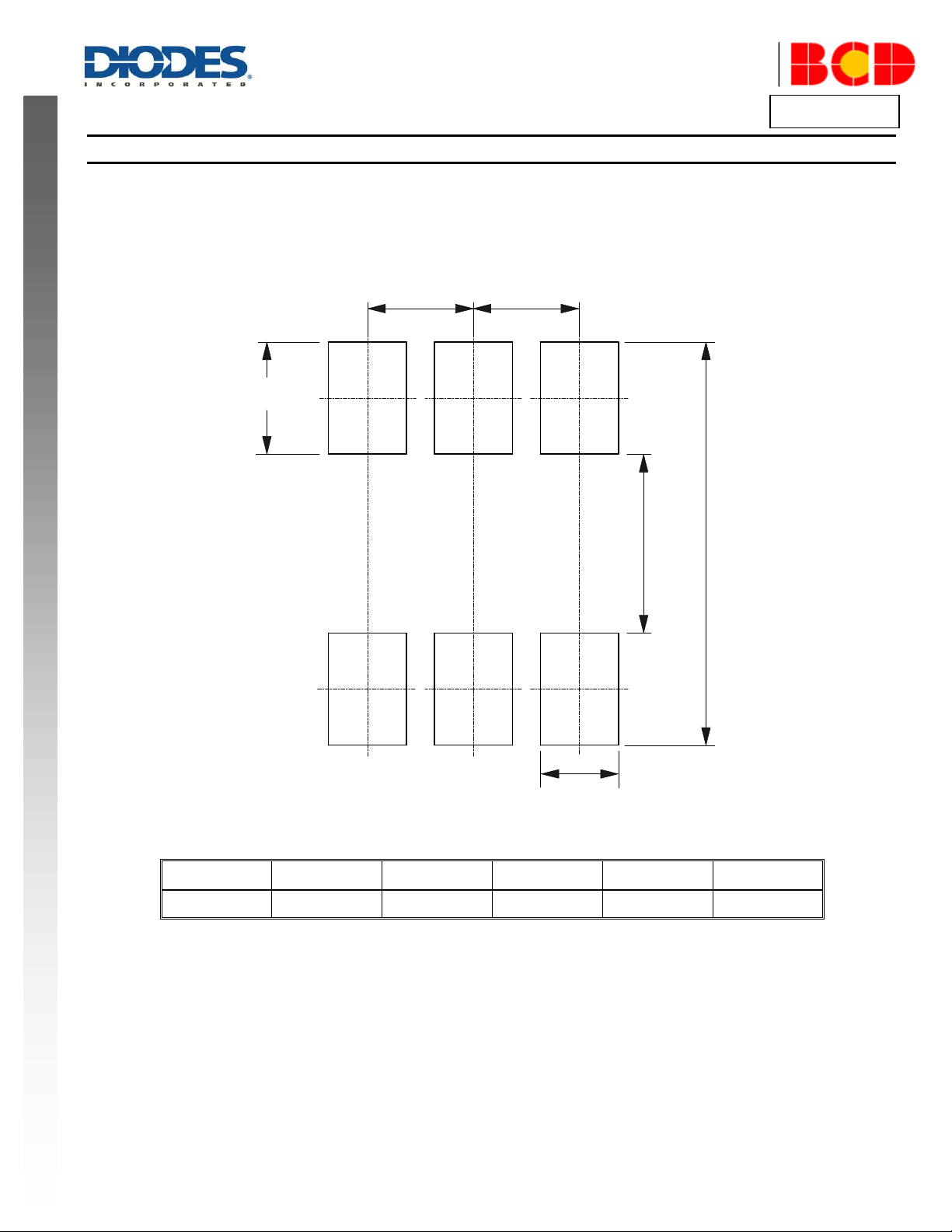
E E
G
Z
Y
X
Dimensions
Z
(mm)/(inch)
G
(mm)/(inch)
X
(mm)/(inch)
Y
(mm)/(inch)
E
(mm)/(inch)
Value
3.600/0.142
1.600/0.063
0.700/0.028
1.000/0.039
0.950/0.037
Suggested Pad Layout
(1) Package Type: SOT26
Page 11
AP3036B
Document number: DS37004 Rev. 1 - 2
11 of 11
www.diodes.com
March 2014
© Diodes Incorporated
AP3036B
A Product Line of
Diodes Incorporated
NE W P R OD U C T
DIODES INCORPORATED MAKES NO WARRANTY OF ANY KIND, EXPRESS OR IMPLIED, WITH REGARDS TO THIS DºC UMENT,
INCLUDING, BUT NOT LIMITED TO, THE IMPLIED WARRANTIES OF MERCHANTABILITY AND FITNESS FOR A PARTICULAR PURPOSE
(AND THEIR EQUIVALENTS UNDER THE LAWS OF ANY JURISDICTION).
Diodes Incorporated and its subsidiaries reserve the right to make modifications, enhancements, improvements, corrections or other changes
without further notice to this document and any product described herein. Diodes Incorporated does not assume any liability arising out of the
application or use of this document or any product described herein; neither does Diodes Incorporated convey any license under its patent or
trademark rights, nor the rights of others. Any Customer or user of this document or products described herein in such applications shall assume
all risks of such use and will agree to hold Diodes Incorporated and all the companies whose products are represented on Diodes Incorporated
website, harmless against all damages.
Diodes Incorporated does not warrant or accept any liability whatsoever in respect of any products purchased through unauthorized sales channel.
Should Customers purchase or use Diodes Incorporated products for any unintended or unauthorized application, Customers shall indemnify and
hold Diodes Incorporated and its representatives harmless against all claims, damages, expenses, and attorney fees arising out of, directly or
indirectly, any claim of personal injury or death associated with such unintended or unauthorized application.
Products described herein may be covered by one or more United States, international or foreign patents pending. Product names and markings
noted herein may also be covered by one or more United States, international or foreign trademarks.
This document is written in English but may be translated into multiple languages for reference. Only the English version of this document is the
final and determinative format released by Diodes Incorporated.
Diodes Incorporated products are specifically not authorized for use as critical components in life support devices or systems without the express
written approval of the Chief Executive Officer of Diodes Incorporated. As used herein:
A. Life support devices or systems are devices or systems which:
1. are intended to implant into the body, or
2. support or sustain life and whose failure to perform when properly used in accordance with instructions for use provided in the
labeling can be reasonably expected to result in significant injury to the user.
B. A critical component is any component in a life support device or system whose failure to perform can be reasonably expected to cause the
failure of the life support device or to affect its safety or effectiveness.
Customers represent that they have all necessary expertise in the safety and regulatory ramifications of their life support devices or systems, and
acknowledge and agree that they are solely responsible for all legal, regulatory and safety-related requirements concerning their products and any
use of Diodes Incorporated products in such safety-critical, life support devices or systems, notwithstanding any devices- or systems-related
information or support that may be provided by Diodes Incorporated. Further, Customers must fully indemnify Diodes Incorporated and its
representatives against any damages arising out of the use of Diodes Incorporated products in such safety-critical, life support devices or systems.
Copyright © 2014, Diodes Incorporated
www.diodes.com
IMPORTANT NOTICE
LIFE SUPPORT
 Loading...