

Page 1
Data Sheet
WHITE LED STEP-UP CONVERTER AP3031
General Description
The AP3031 is an inductor-based DC/DC boost converter designed to drive LED arrays. 1.4A switching
current allows AP3031 to be used in different 7' to 10'
LCD panel backlights (3*13 LED arrays typically).
A constant frequency 1MHz PWM control scheme is
employed in this IC, which means tiny external components can be used. Specifically, 1mm tall 4.7
inductor and 0.47
application is sufficient.
The over output voltage protection is equipped in
AP3031, which protects the IC under open load condition. The AP3031 includes UVLO, soft-start, current
limit and OTSD to protect the circuit.
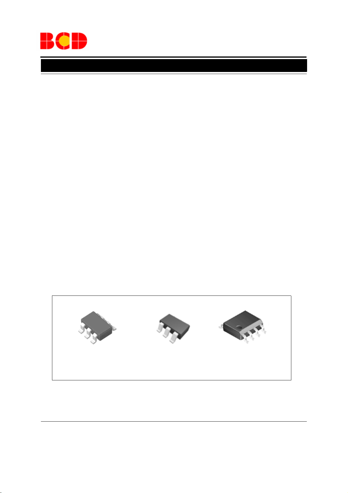
The AP3031 is available in standard SOT-23-6, TSOT23-6 and SOIC-8 packages.
μF output capacitor for the typical
μH
Features
· Up to 92% Efficiency
(V
· Up to 84% Efficiency
(V
· Fast 1MHz Switching Frequency
· Wide Input Voltage Range: 2.7V to 16V
· Low 200mV Feedback Voltage
· Output Over Voltage Protection
· Cycle by Cycle Current Limit: 1.4A
· Built-in Soft-start
· Built-in Standby Mode to Achieve High Fre-
· Built-in Thermal Shutdown Function
· Under Voltage Lockout
=9V, I
IN
=5V, I
IN
quency PWM Dimming
OUT
OUT
=260mA)
=260mA)
Applications
· 7' to 10' LCD Panels
· Digital Photo Frame
· GPS Receiver
· EPC
· PDVD
SOT-23-6 TSOT-23-6 SOIC-8
Figure 1. Package Types of AP3031
Dec. 2012 Rev. 1. 6 BCD Semiconductor Manufacturing Limited
1
Page 2
Data Sheet
1
2
3
4
8
7
6
5
1
2
34
5
Pin 1 Mark
6
WHITE LED STEP-UP CONVERTER AP3031
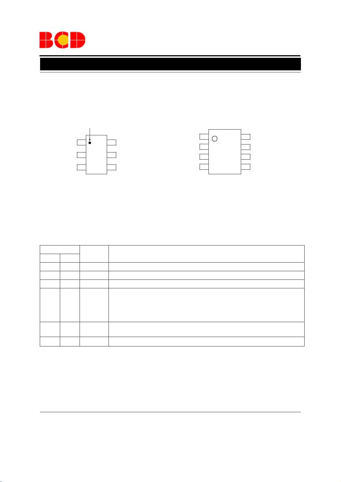
Pin Configuration
K/KT Package
(SOT-23-6/TSOT-23-6)
SW
GND
FB
V
IN
OV
CTRL
FB
GND
GND
SW
M Package
(SOIC-8)
CTRL
OV
GND
V
IN
Figure 2. Pin Configuration of AP3031 (Top View)
Pin Description
Pin Number
6-Pin 8-Pin
1 4 SW Switch Pin. Connect external inductor and Schottky
2 2, 3, 6 GND Ground Pin
3 1 FB Voltage Feedback Pin. Reference voltage is 200mV
4
5 7 OV Over-voltage Protection Input Pin. Connect to the output directly. On OVP condition, the out-
65 V
Pin Name Function
Enable and Dimming Control Pin. Connect to a high input to enable the IC or a low input to
disable the IC.
8CTRL
If logic low time is more than about 0.7ms and then enable the IC, the AP3031 will soft start to
protect system departments. If logic low time is less than about 0.7ms and then enable the IC,
the AP3031 will hold on standby mode and start directly to achieve high frequency dimming
put voltage will be clamped
Input Supply Pin. Must be locally bypassed
IN
Dec. 2012 Rev. 1. 6 BCD Semiconductor Manufacturing Limited
2
Page 3
Data Sheet
Q1
Σ
A2
A1
1MHz
OSCILLATOR
RAMP
GENERATOR
V
REF
DRIVER
1.25 V
COMPARATOR
200 mV
SOFT
START
V
IN
CTRL
FB
GND
SW
STANDBY
OV
To Control
Logic
CONTROL
LOGIC
OVER
TEMPERATURE
DETECTOR
OV
WHITE LED STEP-UP CONVERTER AP3031
Functional Block Diagram
3 (1)
6 (5)
4 (8)
A (B)
A SOT-23-6/TSOT-23-6
B SOIC-8
1 (4)
5 (7)
2
(2, 3, 6)
Figure 3. Functional Block Diagram of AP3031
Ordering Information
AP3031 -
Circuit Type
Package
K: SOT-23-6
KT: TSOT-23-6
M: SOIC-8
Temperature
Range
o
-40 to 85
C
Part Number Marking ID Packing Type
AP3031KTR-G1 GEC Tape & Reel
AP3031M-G1 3031M-G1 Tube
AP3031MTR-G1 3031M-G1 Tape & Reel
3
Package
SOT-23-6
TSOT-23-6 AP3031KTTR-G1 L1E Tape & Reel
SOIC-8
BCD Semiconductor's Pb-free products, as designated with "G1" suffix in the part number, are RoHS compliant and green.
Dec. 2012 Rev. 1. 6 BCD Semiconductor Manufacturing Limited
G1: Green
TR: Tape and Reel
Blank: Tube
Page 4
Data Sheet
WHITE LED STEP-UP CONVERTER AP3031
Absolute Maximum Ratings (Note 1)
Parameter Symbol Value Unit
Input Voltage V
SW Voltage V
FB Voltage V
CTRL Voltage V
Thermal Resistance
(Junction to Ambient, No Heat Sink) θ
Operating Junction Temperature T
Storage Temperature Range T
Lead Temperature (Soldering, 10sec) T
LEAD
IN
SW
FB
CTRL
JA
J
STG
SOT-23-6/TSOT-23-6 265
SOIC-8 120
20 V
38 V
20 V
20 V
150
-65 to 150
260
o
C/W
o
C
o
C
o
C
ESD (Machine Model) 600 V
ESD (Human Body Model) 4000 V
Note 1: Stresses greater than those listed under "Absolute Maximum Ratings" may cause permanent damage to the device.
These are stress ratings only, and functional operation of the device at these or any other conditions beyond those indicated
under "Recommended Operating Conditions" is not implied. Exposure to "Absolute Maximum Ratings" for extended periods
may affect device reliability.
Recommended Operating Conditions
Parameter Symbol Min Max Unit
Operating Temperature Range T
Input Voltage V
CTRL Voltage V
-40 85
OP
IN
CTRL
2.7 16
16 V
Dec. 2012 Rev. 1. 6 BCD Semiconductor Manufacturing Limited
4
o
C
V
Page 5
Data Sheet
WHITE LED STEP-UP CONVERTER AP3031
Electrical Characteristics
(VIN=5.0V, V
=5.0V, TA=25oC, unless otherwise specified.)
CTRL
Parameter Symbol Conditions Min Typ Max Unit
Operating Voltage V
Feedback Voltage (Note 2)
FB Pin Bias Current I
Quiescent Current I
Shutdown Quiescent Current I
IN
V
FB
FB
Q
SHDN
I
=20mA, 3 LEDs,
OUT
T
=-40oC to 85oC
A
VFB=VIN, no switching 3.0 4.0 5.0 mA
V
=0V 20 50 80 μA
CTRL
2.7 16
188 200 212 mV
35 100 nA
Switching Frequency f 0.75 1 1.3 MHz
Maximum Duty Cycle D
Switch Current Limit (Note 3) I
Switch V
Saturation Voltage V
CE
MAX
LIMIT
CESATISW
Switch Leakage Current V
CTRL Pin Voltage
V
CTRL
D=60% 1.2 1.4 A
=0.6A 300 mV
=16V 0.01 5 μA
SW
Active high 1.8
90 93 %
Active low 0.5
CTRL Pin Bias Current I
CTRL
35 60 85 μA
V
V
OVP Voltage V
Soft-start Time t
Standby Time t
Thermal Shutdown T
Thermal Resistance
(Junction to Case)
OVP
SS
STB
OTSD
θ
JC
15.5 17.5 19.5 V
250 μs
0.7 ms
155
60
o
o
C/W
C
Note 2: The bold type specifications of full temperature range are guaranteed by design (GBD).
Note 3: The switch current limit is related to duty cycle. Please refer to Figure 15 for detail.
Dec. 2012 Rev. 1. 6 BCD Semiconductor Manufacturing Limited
5
Page 6
Data Sheet
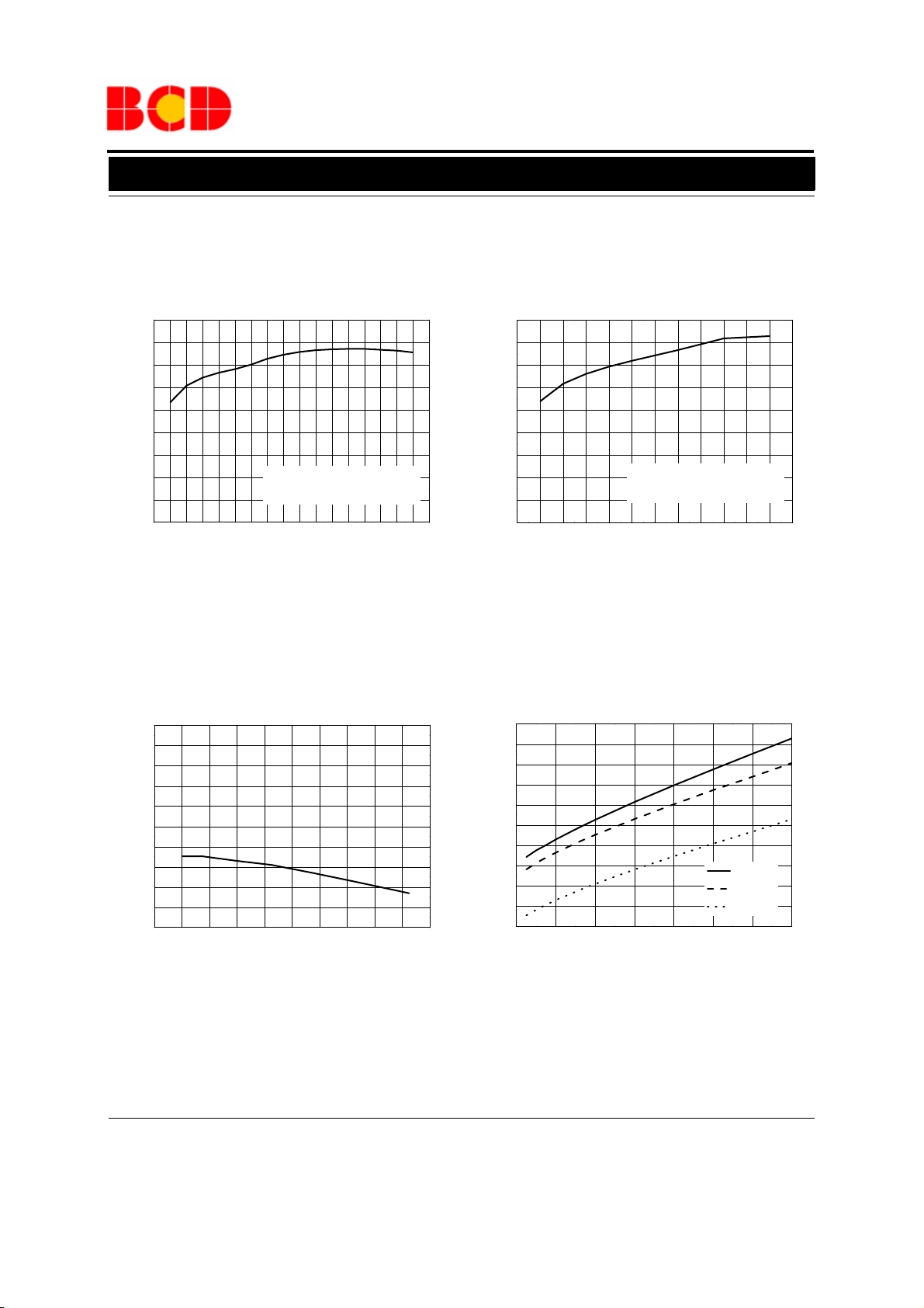
0 20 40 60 80 100 120 140 160 180 200 220 240 260 280 300 320 340
45
50
55
60
65
70
75
80
85
90
Efficiency (%)
Output Current (mA)
VIN=5V, V
OUT
=10V, TA=25oC
C
IN
=10μF, C
OUT
=0.47μF, L=4.7μH
3.54.04.55.05.56.06.57.07.58.08.59.09.5
50
55
60
65
70
75
80
85
90
95
Efficiency (%)
Input Voltage (V)
V
OUT
=10V, I
OUT
=260mA,TA=25oC
C
IN
=10μF, C
OUT
=0.47μF, L=4.7μH
-60 -40 -20 0 20 40 60 80 100 120 140
2.20
2.25
2.30
2.35
2.40
2.45
2.50
2.55
2.60
2.65
2.70
Minimum Operating Voltage (V)
Temperature (oC)
2 4 6 8 10 12 14 16
3.7
3.8
3.9
4.0
4.1
4.2
4.3
4.4
4.5
4.6
4.7
Quiescent Current (mA)
Input Voltage (V)
TA= -40oC
TA= 25oC
TA= 85oC
WHITE LED STEP-UP CONVERTER AP3031
Typical Performance Characteristics
(WLED forward voltage (VF)=3.2V at IF=20mA, unless otherwise noted.)
Figure 4. Efficiency vs. Output Current Figure 5. Efficiency vs. Input Voltage
Figure 6. Minimum Operating Voltage vs. Temperature Figure 7. Quiescent Current vs. Input Voltage
Dec. 2012 Rev. 1. 6 BCD Semiconductor Manufacturing Limited
6
Page 7

Data Sheet
2 4 6 8 10 12 14 16
40
45
50
55
60
65
70
75
80
85
Shutdown Quiescent Current (μA)
Input Voltage (V)
TA= -40oC
TA= 25oC
TA= 85oC
-60 -40 -20 0 20 40 60 80 100 120 140
0.4
0.6
0.8
1.0
1.2
1.4
1.6
1.8
2.0
CTRL Pin Voltage (V)
Temperature (oC)
2 4 6 8 1012141618
20
40
60
80
100
120
140
160
180
200
220
CTRL Pin Current (μA)
CTRL Pin Voltage (V)
-60 -40 -20 0 20 40 60 80 100 120 140
188
190
192
194
196
198
200
202
204
206
208
210
212
Feedback Voltage (mV)
Temperature (oC)
I
OUT
= 20mA
WHITE LED STEP-UP CONVERTER AP3031
Typical Performance Characteristics (Continued)
(WLED forward voltage (VF)=3.2V at IF=20mA, unless otherwise noted.)
Figure 8. Shutdown Quiescent Current vs. Input Voltage
Figure 10. CTRL Pin Current vs. CTRL Pin Voltage
Dec. 2012 Rev. 1. 6 BCD Semiconductor Manufacturing Limited
Figure 9. CTRL Pin Voltage vs. Temperature
Figure 11. Feedback Voltage vs. Temperature
7
Page 8

Data Sheet
-60 -40 -20 0 20 40 60 80 100 120 140
0.6
0.7
0.8
0.9
1.0
1.1
1.2
1.3
1.4
Frequency (MHz)
Temperature (oC)
-60 -40 -20 0 20 40 60 80 100 120 140
14
15
16
17
18
19
20
OVP Voltage (V)
Temperature (oC)
2 4 6 8 1012 141618
0.70
0.75
0.80
0.85
0.90
0.95
1.00
1.05
1.10
1.15
1.20
Frequency (MHz)
Input Voltage (V)
10 20 30 40 50 60 70 80 90
1.0
1.1
1.2
1.3
1.4
1.5
1.6
1.7
1.8
1.9
2.0
Switch Current Limit (A)
Duty Cycle (%)
TA=-40oC
TA=25oC
TA=85oC
WHITE LED STEP-UP CONVERTER AP3031
Typical Performance Characteristics (Continued)
(WLED forward voltage (VF)=3.2V at IF=20mA, unless otherwise noted.)
Figure 12. Frequency vs. Temperature
Figure 14. Frequency vs. Input Voltage
Dec. 2012 Rev. 1. 6 BCD Semiconductor Manufacturing Limited
Figure 13.
OVP Voltage vs. Temperature
Figure 15. Switch Current Limit vs. Duty Cycle
8
Page 9

Data Sheet
0.0 0.1 0.2 0.3 0.4 0.5 0.6 0.7 0.8 0.9 1.0 1.1
0
50
100
150
200
250
300
350
400
450
500
550
600
650
Switch Saturation Voltage (mV)
Switch Current (A)
TA=-40oC
TA=25oC
TA=85oC
0 20 40 60 80 100 120 140 160 180 200 220 240 260 280 300 320 340
30
35
40
45
50
55
60
65
70
75
80
Case Temperature (
o
C)
Output Current (mA)
VIN=5V, V
OUT
=10V, TA=25oC
C
IN
=10μF, C
OUT
=0.47μF, L=4.7μH
WHITE LED STEP-UP CONVERTER AP3031
Typical Performance Characteristics (Continued)
(WLED forward voltage (VF)=3.2V at IF=20mA, unless otherwise noted.)
Figure 16. Switch Saturation Voltage
vs. Switch Current
Dec. 2012 Rev. 1. 6 BCD Semiconductor Manufacturing Limited
Figure 17. Case Temperature vs. Output Current
9
Page 10

Data Sheet
LED
ISET
I
mV200
R =
>0.7ms
<0.7ms
WHITE LED STEP-UP CONVERTER AP3031
Application Information
Operation
The AP3031 is a boost DC-DC converter which uses a
constant frequency, current mode control scheme to
provide excellent line and load regulation. Operation
can be best understood by referring to Figure 3 and
Figure 24.
At the start of each oscillator cycle, switch Q1 turns on.
The switch current will increase linearly. The voltage
on sense resistor is proportional to the switch current.
The output of the current sense amplifier is added to a
stabilizing ramp and the result is fed into the noninversion input of the PWM comparator A2. When this
voltage exceeds the output voltage level of the error
amplifier A1, the switch is turned off.
It is clear that the voltage level at inversion input of A2
sets the peak current level to keep the output in
regulation. This voltage level is the output signal of
error amplifier A1, and is the amplified signal of the
voltage difference between feedback voltage and
reference voltage of 200mV. So, a constant output
current can be provided by this operation mode.
LED Current Control
Refer to Figure 24, the LED current is controlled by the
feedback resistor R
determined by the feedback voltage and resistor R
so the precise resistors are preferred. The resistance of
is in inverse proportion to the LED current since
R
ISET
the feedback reference is fixed at 200mV. The relation
for R
and LED current (I
ISET
below:
. LEDs' current accuracy is
ISET
)can be expressed as
LED
ISET
Soft Start
The AP3031 has an internal soft start circuit to limit
the inrush current during startup. If logic low time on
CTRL pin is more than about 0.7ms and then enable
the IC, the AP3031 will start smoothly to protect the
supplier. The time of startup is controlled by internal
soft-start capacitor. Details please refer to Figure 18.
V
CTRL
5V/div
V
SW
5V/div
I
L
500mA/div
V
OUT
10V/div
Time 80μs/div
Figure 18. Soft-start Waveform
V
=5V, 3×13 LEDs, I
IN
LED
=260mA
Standby and Dimming
To avoid audio noise and achieve high frequency dimming, AP3031 is equipped with standby function. If
logic low time on CTRL pin is less than about 0.7ms
and then enable the IC, the AP3031 will hold on
standby mode and start directly to achieve high frequency dimming. Details please refer to Figure 19.
,
V
CTRL
5V/div
V
SW
5V/div
I
L
500mA/div
V
OUT
10V/div
Time 80μs/div
Over Voltage Protection
The AP3031 has an internal open load protection
circuit. When the LEDs are disconnected from circuit
or fail open, the output voltage is clamped at about
17.5V. The AP3031 will switch at a low frequency, and
minimize current to avoid input voltage drop.
Dec. 2012 Rev. 1. 6 BCD Semiconductor Manufacturing Limited
Figure 19. Standby Waveform
Two typical types of dimming control circuit are
present as below. First, controlling CTRL Pin voltage
to change operation state is a good choice. Second,
10
Page 11

Data Sheet
R1
FB
AP3031
R2R3
V
DC
Effective
Feedback Voltage
R1
FB
AP3031
R2
R3
PWM
R4
C
Effective
Feedback Voltage
AP3031
CTRL
WHITE LED STEP-UP CONVERTER AP3031
Application Information (Continued)
changing the feedback voltage to get appropriate duty
and luminous intensity is also useful.
(1) Adding a Control Signal to CTRL Pin
Adding a PWM signal to CTRL pin directly, the
AP3031 is turned on and off by this signal. When the
PWM frequency is lower than 1kHz(Typ.), the IC
works in the soft-start mode to dimming the light. On
contrary, when the PWM frequency is higher than
1kHz(Typ.), the IC works in the standby mode: the
converter ceaselessly switches off and directly starts to
achieve light dimming. This standby function allows
AP3031 to support high frequency dimming (up to
25kHz or higher) to avoid audio noise. More details
please refer to Figure 20 and Figure 21.
Figure 20. Dimming Control
Using a PWM Signal in CTRL Pin
Comparing with all kinds of PWM signal control, this
method features a stable output voltage and LEDs
current. Please refer to Figure 22.
Using DC Voltage
Figure 22. Dimming Control
Second, using a filtered PWM signal can do it. The
filtered PWM signal can be considered as a varying
and adjustable DC voltage, please refer to Figure 23.
V
CTRL
2.5V/div
V
SW
5V/div
I
L
500mA/div
Using Filtered PWM Voltage
Time 20μs/div
Figure 23. Dimming Control
Figure 21. High Frequency (25kHz)
Dimming Waveform
(2) Changing the Effective Feedback Voltage
There are two popular methods to change the effective
feedback voltage.
First, adding a constant DC voltage through a resistor
divider to FB pin can control the dimming. Changing
the DC voltage or resistor between the FB Pin and the
DC voltage can get appropriate luminous intensity.
Dec. 2012 Rev. 1. 6 BCD Semiconductor Manufacturing Limited
11
Page 12

Data Sheet
FB
AP3031
GND
V
IN
SW
CTRL
C
IN
10
μF
C
OUT
0.47μF
V
IN
5V
V
OUT
L4.7μH
R
ISET
3*13
On /Off
D
OV
L1
D1
C
IN
R3
R4
R2
R1
V
IN
SW
CTRL
GND
FB
OV
V
IN
12V
V
OUT
18V
C
OUT
AP3031
WHITE LED STEP-UP CONVERTER AP3031
Typical Application
3×13 WLEDs
Booster for LNB Application (Note 4)
Dec. 2012 Rev. 1. 6 BCD Semiconductor Manufacturing Limited
12
Page 13

Data Sheet
L1
AP3031
D1
C
IN
R2
R1
VIN
SW
CTRL
GND
FB
OV
V
IN
3.6 V
V
OUT
5V
C
OUT
WHITE LED STEP-UP CONVERTER AP3031
Typical Application
Note 4: V
=(1+R1/R2)*V
OUT
(Continued)
Booster for Portable Charger Application (Note 4)
FB
Figure 24. Typical Application of AP3031
Dec. 2012 Rev. 1. 6 BCD Semiconductor Manufacturing Limited
13
Page 14

Data Sheet
2.820(0.111)
3.020(0.119)
2.650(0.104)
2.950(0.116)
1.500(0.059)
1.700(0.067)
0.950(0.037)TYP
1.800(0.071)
2.000(0.079)
0.300(0.012)
0.400(0.016)
0.700(0.028)REF
0.100(0.004)
0.200(0.008)
0°
8°
0.200(0.008)
0.300(0.012)
0.600(0.024)
0.000(0.000)
0.150(0.006)
0.900(0.035)
1.300(0.051)
1.450(0.057)
MAX
123
4
5
6
Pin 1 Mark
WHITE LED STEP-UP CONVERTER AP3031
Mechanical Dimensions
SOT-23-6 Unit: mm(inch)
Dec. 2012 Rev. 1. 6 BCD Semiconductor Manufacturing Limited
14
Page 15

Data Sheet
2.800(0.110)
3.000(0.118)
1.500(0.059)
1.700(0.067)
2.600(0.102)
3.000(0.118)
0.950(0.037)
BSC
1.900(0.075)
BSC
0.700(0.028)
0.900(0.035)
0.000(0.000)
0.100(0.004)
0.350(0.014)
0.510(0.020)
0
8
°
0.370(0.015)
MIN
0.100(0.004)
0.250(0.010)
°
0.250(0.010)
BSC
GAUGE
PLANE
R0.100(0.004)
MIN
Pin 1 Mark
1.000(0.039)
MAX
WHITE LED STEP-UP CONVERTER AP3031
Mechanical Dimensions (Continued)
TSOT-23-6 Unit: mm(inch)
Dec. 2012 Rev. 1. 6 BCD Semiconductor Manufacturing Limited
15
Page 16

Data Sheet
0
°
8
°
1°
5°
R
0
.
1
5
0
(
0
.
0
0
6
)
R0.150(0.006)
1.000(0.039)
0.330(0.013)
0.510(0.020)
1.350(0.053)
1.750(0.069)
0.100(0.004)
0.300(0.012)
0.900(0.035)
0.800(0.031)
0.200(0.008)
3.800(0.150)
4.000(0.157)
7
°
7
°
2
0
:
1
D
1.270(0.050)
TYP
0.190(0.007)
0.250(0.010)
8
°
D
5.800(0.228)
6.200(0.244)
0.675(0.027)
0.725(0.029)
0.320(0.013)
8
°
0.450(0.017)
0.800(0.031)
4.700(0.185)
5.100(0.201)
Note: Eject hole, oriented hole and mold mark is optional.
WHITE LED STEP-UP CONVERTER AP3031
Mechanical Dimensions (Continued)
SOIC-8 Unit: mm(inch)
Dec. 2012 Rev. 1. 6 BCD Semiconductor Manufacturing Limited
16
Page 17

BCD Semiconductor Manufacturing Limited
IMPORTANT NOTICE
http://www.bcdsemi.com
BCD Semiconductor Manufacturing Limited reserves the right to make changes without further notice to any products or specifications herein. BCD Semiconductor Manufacturing Limited does not assume any responsibility for use of any its products for any
IMPORTANT NOTICE
IMPORTANT NOTICE
particular purpose, nor does BCD Semiconductor Manufacturing Limited assume any liability arising out of the application or use
of any its products or circuits. BCD Semiconductor Manufacturing Limited does not convey any license under its patent rights or
BCD Semiconductor Manufacturing Limited reserves the right to make changes without further notice to any products or specifi-
BCD Semiconductor Manufacturing Limited reserves the right to make changes without further notice to any products or specifi-
other rights nor the rights of others.
cations herein. BCD Semiconductor Manufacturing Limited does not assume any responsibility for use of any its products for any
cations herein. BCD Semiconductor Manufacturing Limited does not assume any responsibility for use of any its products for any
particular purpose, nor does BCD Semiconductor Manufacturing Limited assume any liability arising out of the application or use
particular purpose, nor does BCD Semiconductor Manufacturing Limited assume any liability arising out of the application or use
MAIN SITE
of any its products or circuits. BCD Semiconductor Manufacturing Limited does not convey any license under its patent rights or
of any its products or circuits. BCD Semiconductor Manufacturing Limited does not convey any license under its patent rights or
- Headquarters
BCD (Shanghai) Micro-electronics Limited
other rights nor the rights of others.
other rights nor the rights of others.
No. 1600, Zi Xing Road, Shanghai ZiZhu Science-based Industrial Park, 200241, P. R.C.
Tel: +86-021-2416-2266, Fax: +86-021-2416-2277
MAIN SITE
MAIN SITE
REGIONAL SALES OFFICE
- Headquarters
BCD Semiconductor Manufacturing Limited
BCD Semiconductor Manufactur ing Limited
Shenzhen Office
- Wafer Fab
No. 1600, Zi Xing Road, Shanghai ZiZhu Science-based Industrial Park, 200241, China
Shanghai SIM-BCD Semiconductor Manufacturing Co., Ltd., Shenzhen Office
Shanghai SIM-BCD Semiconductor Manufacturing Limited
Tel: +86-21-24162266, Fax: +86-21-24162277
Unit A Room 1203,Skyworth Bldg., Gaoxin Ave.1.S., Nanshan District
800, Yi Shan Road, Shanghai 200233, China
Shenzhen 518057, China
Tel: +86-21-6485 1491, Fax: +86-21-5450 0008
REGIONAL SALES OFFICE
Tel: +86-0755-8660-4900, Fax: +86-0755-8660-4958
Shenzhen Office
REGIONAL SALES OFFICE
Shanghai SIM-BCD Semiconductor Manufacturing Co., Ltd., Shenzhen Office
Taiwan Office (Hsinchu)
Shenzhen Office
Unit A Room 1203, Skyworth Bldg., Gaoxin Ave.1.S., Nanshan District, Shenzhen,
BCD Semiconductor (Taiwan) Company Limited
Shanghai SIM-BCD Semiconductor Manufacturing Co., Ltd. Shenzhen Office
China
8F, No.176, Sec. 2, Gong-Dao 5th Road, East District
Advanced Analog Circuits (Shanghai) Corporation Shenzhen Office
Tel: +86-755-8826 7951
HsinChu City 300, Taiwan, R.O.C
Room E, 5F, Noble Center, No.1006, 3rd Fuzhong Road, Futian District, Shenzhen 518026, China
Fax: +86-755-8826 7865
Tel: +886-3-5160181, Fax: +886-3-5160181
Tel: +86-755-8826 7951
Fax: +86-755-8826 7865
- Wafer Fab
Shanghai SIM-BCD Semiconductor Manufacturing Co., Ltd.
800 Yishan Road, Shanghai 200233, China
Tel: +021-6485-1491, Fax: +86-021-5450-0008
- Wafer Fab
BCD Semiconductor Manufacturing Limited
Shanghai SIM-BCD Semiconductor Manufacturing Co., Ltd.
Taiwan Office (Taipei)
- IC Design Group
800 Yi Shan Road, Shanghai 200233, China
BCD Semiconductor (Taiwan) Company Limited
Advanced Analog Circuits (Shanghai) Corporation
Tel: +86-21-6485 1491, Fax: +86-21-5450 0008
3F, No.17, Lane 171, Sec. 2, Jiu-Zong Rd., Nei-Hu Dist., Taipei(114), Taiwan, R.O.C
8F, Zone B, 900, Yi Shan Road, Shanghai 200233, China
Tel: +886-2-2656 2808
Tel: +86-21-6495 9539, Fax: +86-21-6485 9673
Fax: +886-2-2656-2806/26562950
Taiwan Office
BCD Semiconductor (Taiwan) Company Limited
USA Office
Taiwan Office
4F, 298-1, Rui Guang Road, Nei-Hu District, Taipei,
BCD Semiconductor Corp.
BCD Semiconductor (Taiwan) Company Limited
Tai wan
48460 Kato Road, Fremont, CA 94538, USA
4F, 298-1, Rui Guang Road, Nei-Hu District, Taipei,
Tel: +886-2-2656 2808
Tel: +1-510-668-1950
Taiwan
Fax: +886-2-2656 2806
Fax: +1-510-668-1990
Tel: +886-2-2656 2808
Fax: +886-2-2656 2806
USA Office
Korea Office
BCD Semiconductor Limited Korea office.
Room 101-1112, Digital-Empire II, 486 Sin-dong,
Yeongtong-Gu, Suwon-city, Gyeonggi-do, Korea
Tel: +82-31-695-8430
BCD Semiconductor Corp.
USA Office
30920 Huntwood Ave. Hayward,
BCD Semiconductor Corporation
CA 94544, USA
30920 Huntwood Ave. Hayward,
Tel : +1-510-324-2988
CA 94544, U.S.A
Fax: +1-510-324-2788
Tel : +1-510-324-2988
Fax: +1-510-324-2788
 Loading...