

Page 1
WHITE LED STEP-UP CONVERTER AP3019A
Data Sheet
General Description
The AP3019A is an inductor-based DC/DC converter
designed to drive up to eight white LEDs in series for
backlight. Only one feedback resistor is needed to
control the LED current and obtain required
brightness.
A constant frequency 1.2MHz PWM control scheme
is employed in this IC, which means tiny external
components can be used. Specifically, 1mm tall
inductor and 0.22µF output capacitor for a typical
application is sufficient. Additionally, the Schottky
diode in boost circuit is integrated on this chip.
AP3019A also provides a disable pin to ease its use
for different systems.
The output over-voltage protection is implemented in
AP3019A. When any LED is broken or in other
abnormal conditions, the output voltage will be
clamped.
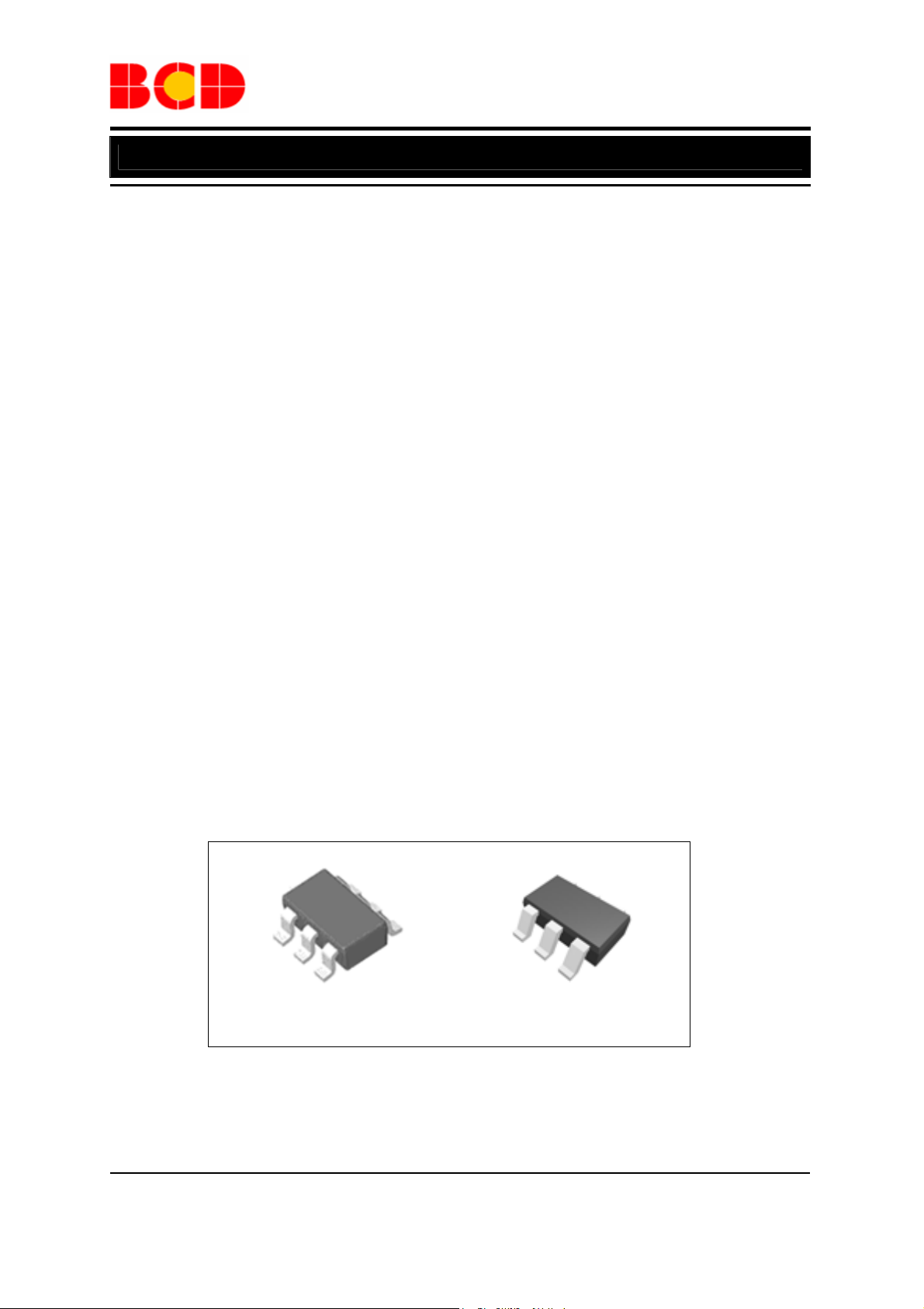
The AP3019A is available in standard SOT-23-6 and
TSOT-23-6 packages.
Features
Inherently Uniform LED Current
•
• High Efficiency up to 84%
• No Need for External Schottky Diode
• Output Over-voltage Protection (OVP)
• Fixed 1.2MHz Switching Frequency
• Uses Tiny 1mm Tall Inductor
• Requires Only 0.22µF Output Capaci t or
Applications
• Cellular Phones
• Digital Cameras
• LCD modules
• GPS Receivers
• PDAs, Handheld Computers
SOT-23-6 TSOT-23-6
Figure 1. Package Types of AP3019A
May. 2010 Rev. 1.8 BCD Semiconductor Manufacturing Limited
1
Page 2
Data Sheet
WHITE LED STEP-UP CONVERTER AP3019A
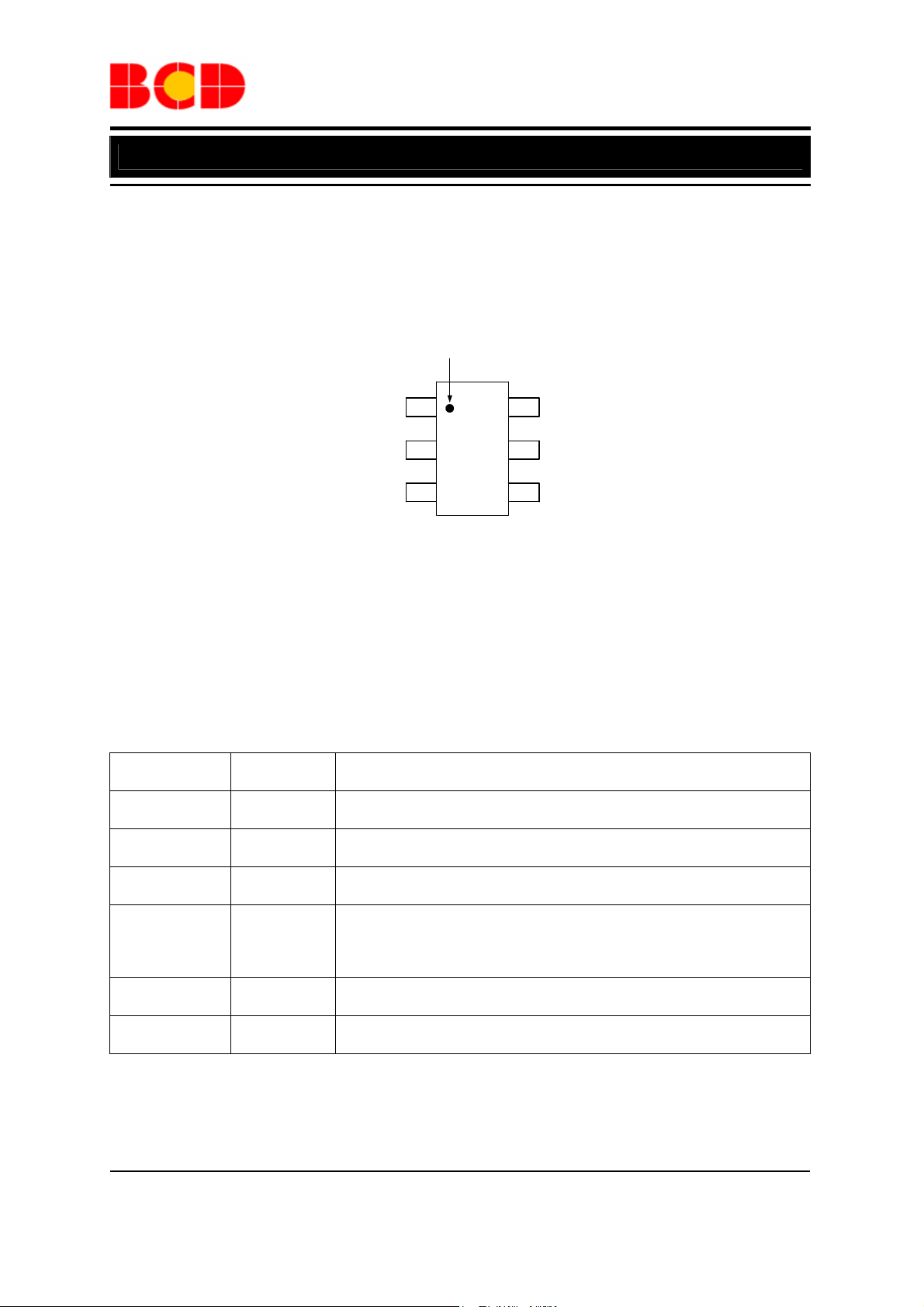
Pin Configuration
K/KT Package
(SOT-23-6/TSOT-23-6)
Pin 1 Dot by Marking
SW
GND
FB
Figure 2. Pin Configuration of AP3019A (Top View)
1
2
34
V
6
5
IN
V
OUT
CTRL
Pin Description
Pin Number Pin Name Function
1 SW
2 GND
3 FB
4 CTRL
5 V
OUT
6 VIN
Switch pin. Connect external inductor
Ground
Voltage feedback pin. Reference voltage is 200mV
Shutdown and dimming pin. Connect to 1.8V or higher to enable
device; Connect to 0.5V or less to disable device; Connect to a PWM
signal to achieve LEDs brightness dimming
Output pin. Connect to the cathode of internal Schottky diode
Input supply pin. Must be connected to a local bypass capacitor
May. 2010 Rev. 1.8 BCD Semiconductor Manufacturing Limited
2
Page 3
Data Sheet
WHITE LED STEP-UP CONVERTER AP3019A
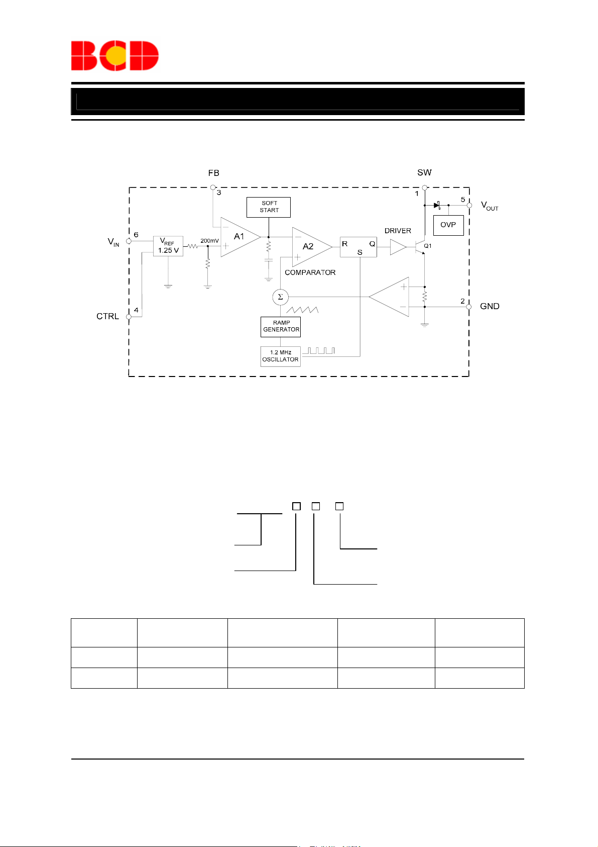
Functional Block Diagram
Figure 3. Functional Block Diagram of AP3019A
Ordering Information
AP3019A -
Circuit Type
Package
K: SOT-23-6 TR: Tape & Reel
KT: TSOT-23-6
Package
SOT-23-6
Temperature
Range
-40 to 85°C
Part Number Marking ID Packing Type
AP3019AKTR-G1 GAS Tape & Reel
G1: Green
TSOT-23-6
-40 to 85°C
AP3019AKTTR-G1 L8E Tape & Reel
BCD Semiconductor's Pb-free products, as designated with "G1" suffix in the part number, are RoHS compliant
and green.
May. 2010 Rev. 1.8 BCD Semiconductor Manufacturing Limited
3
Page 4
Data Sheet
WHITE LED STEP-UP CONVERTER AP3019A
Absolute Maximum Ratings (Note 1)
Parameter Symbol Value Unit
Input Voltage VIN 20 V
SW Pin Voltage VSW 38 V
Feedback Voltage VFB 20 V
CTRL Pin Voltage V
Thermal Resistance (Junction to
Ambient, No Heat Sink)
Operating Junction Temperature TJ 150
Storage Temperature Range T
Lead T em perature (Soldering, 10sec) T
ESD (Machine Model) 250 V
ESD (Human Body Model) 2000 V
20 V
CTRL
θ
JA
-65 to 150
STG
260
LEAD
265
°C/W
°C
°C
°C
Note 1: Stresses greater than those listed under “Absolute Maximum Ratings” may cause permanent damage to
the device. These are stress ratings only, and functional operation of the device at these or any other conditions
beyond those indicated under “Recommended Operating Conditions” is not implied. Exposure to “Absolute
Maximum Ratings” for extended periods may affect device reliability.
Recommended Operating Conditions
Parameter Symbol Min Max Unit
Operating T em perature Range TOP -40 85
Input Voltage VIN 2.5 16 V
CTRL Pin Voltage V
16 V
CTRL
°C
May. 2010 Rev. 1.8 BCD Semiconductor Manufacturing Limited
4
Page 5
Data Sheet
WHITE LED STEP-UP CONVERTER AP3019A
Electrical Characteristics
V
=3V, V
IN
Parameter Symbol Conditions Min Typ Max Unit
Minimum Operating Voltage VIN (min) 2.5
Maximum Operating Voltage VIN (max) 16
Feedback Voltage (Note 2) VFB
FB Pin Bias Current IFB 35 100 nA
Quiescent Current IQ VFB=VIN, no switching 1.5 2.5 3.2 mA
=3V, TA =25°C, unless otherwise specified.
CTRL
=20mA, 4 LEDs,
I
OUT
T
=-40oC to 85oC
A
188 200 212
V
mV
Shutdown Quiescent Current I
V
SHDN
=0V 2.0 4.0 6.0
CTRL
µA
Switching Frequency f 0.9 1.2 1.5 MHz
Maximum Duty Cycle D
90 93 %
MAX
D=40% 550
Switch Current Limit (Note 3) I
LIMIT
mA
D=80% 550
Switch VCE Saturation Voltage V
Switch Leakage Current VSW=5V 0.01 5
ISW=250mA 360 mV
CESAT
µA
High 1.8
CTRL Pin Voltage V
CTRL
V
low 0.5
CTRL Pin Bias Current I
CTRL
100
µA
OVP Voltage VOV 30 V
Schottky Forward Drop V
Schottky Leakage Current
ID=150mA 0.7 V
DROP
VR(reverse voltage)=23V 0.1 4
(reverse voltage)=27V 150
V
R
µA
Soft Start Time t 300
Thermal Resistance
(Junction to Case)
θ
JC
SOT-23-6 60
TSOT-23-6 60
µS
°C/W
Note 2: The bold type specifications of full temperature range are guaranteed by design (GBD).
Note 3: The switch current limit is related to duty cycle. Please refer to Figure 15 for detail.
May. 2010 Rev. 1.8 BCD Semiconductor Manufacturing Limited
5
Page 6

Data Sheet
WHITE LED STEP-UP CONVERTER AP3019A
Typical Performance Characteristics
WLED forward voltage (VF) is 3.45V at IF=20mA, unless otherwise noted.
83
82
81
80
79
78
77
Efficiency (%)
76
75
74
73
-50 -25 0 25 50 75 100
Junction Temperature (oC)
VIN=3.6V, I
CIN=1µF, C
=20mA, 8 LEDs
OUT
=0.22µF, L=22µH
OUT
86
84
82
80
78
Efficiency (%)
76
74
72
70
3.0 3.5 4.0 4.5 5.0
I
=20mA, 8 LEDs,TA=25OC
OUT
CIN=1µF, C
Input Voltage (V)
=0.22µF, L=22µH
OUT
Figure 4. Efficiency vs. Junction Temperature Figure 5. Efficiency vs. Input Voltage
86
85
84
83
82
81
80
Efficiency (%)
79
78
77
76
2345678
VIN=3.6V, I
CIN=1µF, C
LED's Number
=20mA,TA=25OC
OUT
=0.22µF, L=22µH
OUT
Figure 6. Efficiency vs. LED’s Number Figure 7. Schottky Forward Current vs.
350
300
250
200
150
100
Schottky Forward Current (mA)
50
0
0 200 400 600 800 1000
Schottky Forward Drop (mV)
Schottky Forward Drop
May. 2010 Rev. 1.8 BCD Semiconductor Manufacturing Limited
6
Page 7

Data Sheet
WHITE LED STEP-UP CONVERTER AP3019A
Typical Performance Characteristics (Continued)
WLED forward voltage (V
) is 3.45V at IF=20mA, unless otherwise noted.
F
30
25
20
15
10
5
Shutdown Quiescent Current (µA)
0
2 4 6 8 10 12 14 16
Input Voltage (V)
TA=25OC
3.5
3.0
2.5
2.0
1.5
1.0
Quiescent Current (mA)
0.5
0.0
0 2 4 6 8 10 12 14 16
TA=-50OC
TA=25OC
TA=100OC
Input Voltage (V)
Figure 8. Shutdown Quiescent Current vs. Input Voltage Figure 9. Quiescent Current vs. Input Voltage
6.0
5.5
5.0
4.5
4.0
3.5
Input Current (mA)
3.0
2.5
2.0
2.53.03.54.04.55.0
Input Voltage (V)
1.40
1.35
1.30
1.25
1.20
1.15
1.10
Frequency (MHz)
1.05
1.00
0.95
0.90
-50 -25 0 25 50 75 100
Junction Temperature (oC)
Figure 10. Input Current in Output Open Circuit Figure 11. Frequency vs. Junction Temperature
vs. Input Voltage
May. 2010 Rev. 1.8 BCD Semiconductor Manufacturing Limited
7
Page 8

Data Sheet
WHITE LED STEP-UP CONVERTER AP3019A
Typical Performance Characteristics (Continued)
WLED forward voltage (V
) is 3.45V at IF=20mA, unless otherwise noted.
F
210
208
206
204
202
200
198
Feedback Voltage (mV)
196
194
192
190
-50 -25 0 25 50 75 100
Junction Temperature (oC)
0.80
0.78
0.76
0.74
0.72
0.70
0.68
0.66
Schottky Forward Drop (V)
0.64
ID=150mA
0.62
0.60
-50 -25 0 25 50 75 100
Junction Temperature (oC)
Figure 12. Feedback Voltage vs. Figure 13. Schottky Forward Drop vs.
Junction Temperature Junction Temperature
0.50
0.45
0.40
0.35
0.30
0.25
0.20
0.15
Schottky Leakage Current (µA)
0.10
0.05
0.00
-50 -25 0 25 50 75 100
Junction Temperature (oC)
VR=10V
VR=16V
VR=23V
700
600
500
400
300
Current Limit (mA)
200
100
30 40 50 60 70 80 90
Duty Cycle (%)
-50OC
25OC
100OC
Figure 14. Schottky Leakage Current vs. Figure 15. Current Limit vs. Duty Cycle
Junction Temperature
May. 2010 Rev. 1.8 BCD Semiconductor Manufacturing Limited
8
Page 9

Data Sheet
WHITE LED STEP-UP CONVERTER AP3019A
Typical Performance Characteristics (Continued)
WLED forward voltage is 3.45V at I
=20mA, unless otherwise noted.
F
450
400
350
300
250
200
150
Saturation Voltage (mV)
100
50
50 100 150 200 250 300
Switch Current (mA)
1.8
1.7
1.6
1.5
1.4
1.3
1.2
1.1
1.0
0.9
CTRL Pin Voltage (V)
0.8
0.7
0.6
0.5
-50 -25 0 25 50 75 100
Junction Temperature (OC)
Figure 16. Saturation Voltage vs. Switch Current Figure 17. CTRL Pin Voltage vs.
Junction Temperature
Falling Edge
Rising Edge
May. 2010 Rev. 1.8 BCD Semiconductor Manufacturing Limited
9
Page 10

µ
Data Sheet
WHITE LED STEP-UP CONVERTER AP3019A
Application Information
Operation
The AP3019A is a boost DC-DC converter which
uses a constant frequency, current mode control
scheme to provide excellent line and load regulation.
Operation can be best understood by referring to the
Figure 3.
At the start of each oscillator cycle, the SR latch is set
and switch Q1 turns on. The switch current will
increase linearly. The voltage on sense resistor is
proportional to the switch current. The output of the
current sense amplifier is added to a stabilizing ramp
and the result is fed into the non-inversion input of
the PWM comparator A2. When this voltage exceeds
the output voltage level of the error amplifier A1, the
SR latch is reset and the switch is turned off.
It is clear that the voltage level at inversion input of
A2 sets the peak current level to keep the output in
regulation. This voltage level is the output signal of
error amplifier A1, and is the amplified signal of the
voltage difference between feedback voltage and
reference voltage of 200mV. So, a constant output
current can be provided by this operation mode.
Over Voltage Protection
The AP3019A has an internal open-circuit protection
circuit. When the LEDs are disconnected from circuit
or fail open, the output voltage is clamped. The
AP3019A will switch at a low frequency, and
minimize input current.
Soft Start
The AP3019A has an internal soft start circuit to limit
the inrush current during startup. The time of startup
is controlled by internal soft start capacitor. Please
refer to Figure 19.
I
IN
10 0m A/di v
V
OUT
5V /d iv
V
FB
10 0m V/di v
V
CTRL
2V /d iv
Figure 19. Soft Start Waveform
V
IN
Ti me 1 00
=3.6V, 5 LEDs, I
s/ di v
LED
=20mA
Dimming Control
Two typical types of dimming control circuit are
present as below. First, controlling CTRL Pin voltage
to change operation state is a good choice. Second,
Figure 18. Typical Application Circuit to Decide R1
LED Current Control
Refer to Figure 18, the LED current is controlled by
the feedback resistor R1. LEDs' current accuracy is
determined by the regulator's feedback threshold
accuracy and is independent of the LED's forward
voltage variation. So the precise resistors are
preferred. The resistance of R1 is in inverse
proportion to the LED current since the feedback
reference is fixed at 200mV. The relation for R1 and
LED current can be expressed as below:
R =
1
May. 2010 Rev. 1.8 BCD Semiconductor Manufacturing Limited
I
mV200
LED
changing the feedback voltage to get appropriate duty
and luminous intensity is also useful.
(1) Adding a Control Signal to CTRL Pin
Adding a PWM Signal to CTRL pin directly. The
AP3019A is turned on or off by the PWM signal
when it is applied on the CTRL pin. The typical
frequency of this PWM signal can be up to 2kHz.
Please refer to Figure 20.
AP3019A
CTRL
up to 2kHz
Figure 20. Dimming Control Using a PWM Signal in
CTRL Pin
10
Page 11

Data Sheet
WHITE LED STEP-UP CONVERTER AP3019A
Application Information (Continued)
(2) Changing the Effective Feedback Voltage
There are three methods to change the effective
feedback voltage.
First, adding a constant DC voltage through a resistor
divider to FB pin can control the dimming. Changing
the DC voltage or resistor between the FB Pin and the
DC voltage can get appropriate luminous intensity.
Comparing with all kinds of PWM signal control, this
method features a stable output voltage and LEDs
current. Please refer Figure 21.
Third, using a logic signal to change the feedback
voltage. For example, the FB pin is connected to the
GND through a MOSFET and a resistor. And this
MOSFET is controlled a logic signal. The luminous
intensity of LEDs will be changed when the
MOSFET turns on or off.
Figure 21. Dimming Control Using DC Voltage
Second, using a filtered PWM signal can do it. The
filtered PWM signal can be considered as a varying
and adjustable DC voltage.
Figure 22. Dimming Control Using a Filtered PWM
Voltage
Figure 23. Dimming Control Using Logic Signal
May. 2010 Rev. 1.8 BCD Semiconductor Manufacturing Limited
11
Page 12

Data Sheet
WHITE LED STEP-UP CONVERTER AP3019A
Typical Application
C: X5R or X7R dielectric
L: SUMIDA CDRH5D28R-220NC or equivalent
This circuit can work in full temperature
Figure 24. Typical Application of AP3019A
May. 2010 Rev. 1.8 BCD Semiconductor Manufacturing Limited
12
Page 13

Data Sheet
WHITE LED STEP-UP CONVERTER AP3019A
Mechanical Dimensions
SOT-23-6 Unit: mm(inch)
2.820(0.111)
3.020(0.119)
0.300(0.012)
0.400(0.016)
6
Pin 1 Dot by Marking
123
5
4
0.300(0.012)
0.600(0.024)
0.700(0.028)REF
0°
8°
0.200(0.008)
0.950(0.037)TYP
1.800(0.071)
2.000(0.079)
0.000(0.000)
0.150(0.006)
0.900(0.035)
1.300(0.051)
1.450(0.057)
MAX
0.100(0.004)
0.200(0.008)
May. 2010 Rev. 1.8 BCD Semiconductor Manufacturing Limited
13
Page 14

Data Sheet
WHITE LED STEP-UP CONVERTER AP3019A
Mechanical Dimensions (Continued)
TSOT-23-6 Unit: mm(inch)
°
2.800(0.110)
3.000(0.118)
R0.100(0.004)
MIN
0
8
°
1.500(0.059)
1.700(0.067)
0.000(0.000)
0.100(0.004)
0.950(0.037)
BSC
0.700(0.028)
0.900(0.035)
Pin 1 Dot by
Marking
1.900(0.075)
BSC
0.350(0.014)
0.510(0.020)
2.600(0.102)
3.000(0.118)
1.000(0.039)
MAX
GAUGE
PLANE
0.370(0.015)
MIN
0.100(0.004)
0.250(0.010)
0.250(0.010)
BSC
May. 2010 Rev. 1.8 BCD Semiconductor Manufacturing Limited
14
Page 15

BCD Semiconductor Manufacturing Limited
IMPORTANT NOTICE
IMPORTANT NOTICE
BCD Semiconductor Manufacturing Limited reserves the right to make changes without further notice to any products or specifi-
BCD Semiconductor Manufacturing Limited reserves the right to make changes without further notice to any products or specifi-
cations herein. BCD Semiconductor Manufacturing Limited does not assume any responsibility for use of any its products for any
cations herein. BCD Semiconductor Manufacturing Limited does not assume any responsibility for use of any its products for any
particular purpose, nor does BCD Semiconductor Manufacturing Limited assume any liability arising out of the application or use
particular purpose, nor does BCD Semiconductor Manufacturing Limited assume any liability arising out of the application or use
of any its products or circuits. BCD Semiconductor Manufacturing Limited does not convey any license under its patent rights or
of any its products or circuits. BCD Semiconductor Manufacturing Limited does not convey any license under its patent rights or
other rights nor the rights of others.
other rights nor the rights of others.
http://www.bcdsemi.com
MAIN SITE
MAIN SITE
- Headquarters
BCD Semiconductor Manufacturing Limited
BCD Semiconductor Manufactur ing Limited
- Wafer Fab
No. 1600, Zi Xing Road, Shanghai ZiZhu Science-based Industrial Park, 200241, China
Shanghai SIM-BCD Semiconductor Manufacturing Limited
Tel: +86-21-24162266, Fax: +86-21-24162277
800, Yi Shan Road, Shanghai 200233, China
Tel: +86-21-6485 1491, Fax: +86-21-5450 0008
REGIONAL SALES OFFICE
Shenzhen Office
REGIONAL SALES OFFICE
Shanghai SIM-BCD Semiconductor Manufacturing Co., Ltd., Shenzhen Office
Shenzhen Office
Unit A Room 1203, Skyworth Bldg., Gaoxin Ave.1.S., Nanshan District, Shenzhen,
Shanghai SIM-BCD Semiconductor Manufacturing Co., Ltd. Shenzhen Office
China
Advanced Analog Circuits (Shanghai) Corporation Shenzhen Office
Tel: +86-755-8826 7951
Room E, 5F, Noble Center, No.1006, 3rd Fuzhong Road, Futian District, Shenzhen 518026, China
Fax: +86-755-8826 7865
Tel: +86-755-8826 7951
Fax: +86-755-8826 7865
- Wafer Fab
BCD Semiconductor Manufacturing Limited
Shanghai SIM-BCD Semiconductor Manufacturing Co., Ltd.
- IC Design Group
800 Yi Shan Road, Shanghai 200233, China
Advanced Analog Circuits (Shanghai) Corporation
Tel: +86-21-6485 1491, Fax: +86-21-5450 0008
8F, Zone B, 900, Yi Shan Road, Shanghai 200233, China
Tel: +86-21-6495 9539, Fax: +86-21-6485 9673
Taiwan Office
BCD Semiconductor (Taiwan) Company Limited
Taiwan Office
4F, 298-1, Rui Guang Road, Nei-Hu District, Taipei,
BCD Semiconductor (Taiwan) Company Limited
Tai wan
4F, 298-1, Rui Guang Road, Nei-Hu District, Taipei,
Tel: +886-2-2656 2808
Taiwan
Fax: +886-2-2656 2806
Tel: +886-2-2656 2808
Fax: +886-2-2656 2806
USA Office
BCD Semiconductor Corp.
USA Office
30920 Huntwood Ave. Hayward,
BCD Semiconductor Corporation
CA 94544, USA
30920 Huntwood Ave. Hayward,
Tel : +1-510-324-2988
CA 94544, U.S.A
Fax: +1-510-324-2788
Tel : +1-510-324-2988
Fax: +1-510-324-2788
 Loading...