

Page 1
Data Sheet
MICRO POWER STEP-UP DC-DC CONVERTER AP3015/A
General Description
The AP3015/A are Pulse Frequency Modulation
(PFM) DC/DC converters. These two devices are functionally equivalent except the switching current limit.
The AP3015 is designed for higher power systems
with 350mA current limit, and the AP3015A is for
lower power systems with 100mA current limit.
The AP3015/A feature a wide input voltage. The operation voltage is ranged from 1.2Vto 12V (1V to 12V
for AP3015A). A current limited, fixed off-time control scheme conserves operating current, resulting in
high efficiency over a broad range of load current.
They also feature low quiescent current, switching current limiting, low temperature coefficient, etc.
Fewer tiny external components are required in the
applications to save space and lower cost.
Furthermore, to ease its use in differnet systems, a disable terminal is designed to turn on or turn off the chip.
The AP3015/A are available in SOT-23-5 package.
Features
· Low Quiescent Current
In Active Mode (Not Switching): 17
In Shutdown Mode: <1
· Low Operating V
µA
IN
1.2V Typical for AP3015
1.0V Typical for AP3015A
· Low V
CESAT
Switch
200mV Typical at 300mA for AP3015
70mV Typical at 70mA for AP3015A
· High Output Voltage: up to 34V
· Fixed Off-Time Control
· Switching Current Limiting
350mA Typical for AP3015
100mA Typical for AP3015A
· Operating Temperature Range: -40
o
Applications
· MP3, MP4
· Battery Power Supply System
· LCD/OLED Bias Supply
· Handheld Device
· Portable Communication Device
µA Typical
C to 85oC
SOT-23-5
Figure 1. Package Type of AP3015/A
May 2010 Rev. 1. 4 BCD Semiconductor Manufacturing Limited
1
Page 2
Data Sheet
MICRO POWER STEP-UP DC-DC CONVERTER AP3015/A
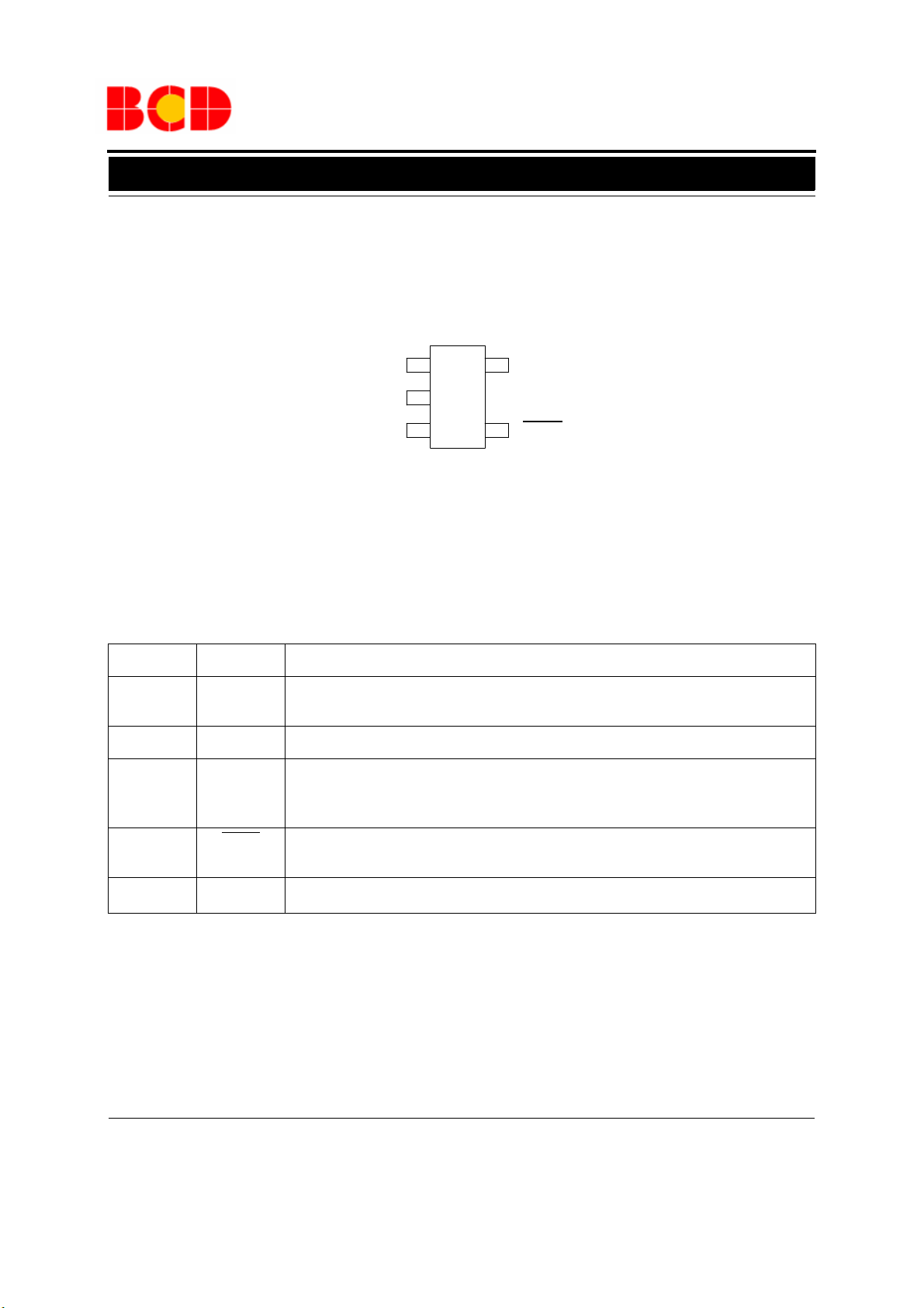
Pin Configuration
K Package
(SOT-23-5)
1
SW
GND
Figure 2. Pin Configuration of AP3015/A (Top View)
2
34
FB
5
V
IN
SHDN
Pin Description
Pin Number Pin Name Function
1 SW Switch Pin. This is the collector of the internal NPN power switch. Minimize the trace area
connected to this Pin to minimize EMI
2 GND Ground Pin. GND should be tied directly to ground plane for best performance
3 FB Feedback Pin. Set the output voltage through this pin. The formula is V
R2). Keep the loop between Vout and FB as short as possible to minimize the ripple and noise,
which is beneficial to the stability and output ripple
OUT
=1.23V*(1+R1/
4 SHDN
5V
IN
Shutdown Control Pin. Tie this pin above 0.9V to enable the device. Tie below 0.25V to turn
off the device
Supply Input Pin. Bypass this pin with a capacitor as close to the device as possible
May 2010 Rev. 1. 4 BCD Semiconductor Manufacturing Limited
2
Page 3
Data Sheet
MICRO POWER STEP-UP DC-DC CONVERTER AP3015/A
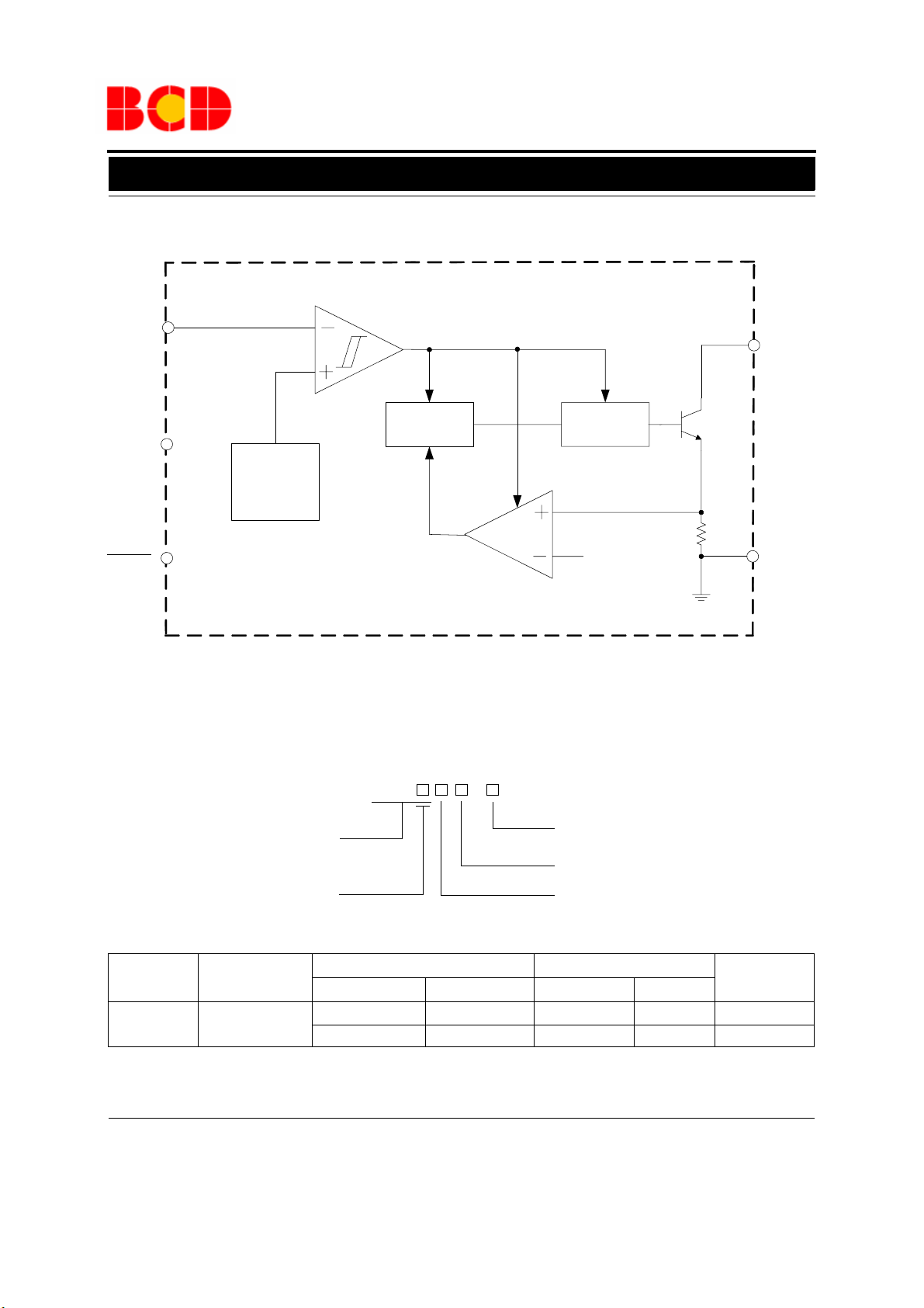
Functional Block Diagram
FEEDBACK
3
FB
COMPARATOR
ENABLE
1
SW
V
V
5
IN
REF
Bandgap
4
SHDN
Ordering Information
Circuit Type
Blank: AP3015
A: AP3015A
400nS
ONE SHOT
RESET
CURRENT-LIMIT
COMPARATOR
Figure 3. Functional Block Diagram of AP3015/A
AP3015
-
DRIVER
CURRENT-LIMIT
REFERENCE
E1: Lead Free
G1: Green
TR: Tape and Reel
Package
K: SOT-23-5
Q1
2
GND
Package
SOT-23-5
BCD Semiconductor's Pb-free products, as designated with "E1" suffix in the part number, are RoHS compliant. Products with
"G1" suffix are available in green package.
Temperature
Range
o
-40 to 85
C
AP3015KTR-E1 AP3015KTR-G1 E6E G6E Tape & Reel
AP3015AKTR-E1 AP3015AKTR-G1 E6F G6F Tape & Reel
Part Number Marking ID
Lead Free Green Lead Free Green
Packing Type
May 2010 Rev. 1. 4 BCD Semiconductor Manufacturing Limited
3
Page 4
Data Sheet
MICRO POWER STEP-UP DC-DC CONVERTER AP3015/A
Absolute Maximum Ratings (Note 1)
Parameter Symbol Value Unit
Input Voltage V
SW Voltage V
FB Voltage V
SHDN
Pin Voltage V
Thermal Resistance (Junction to Ambient, no Heat sink) R
Operating Junction Temperature T
Storage Temperature Range T
Lead Temperature (Soldering, 10sec) T
IN
SW
FB
SHDN
θJA
J
STG
LEAD
15 V
38 V
V
IN
15 V
265
150
-65 to 150
260
o
C/W
V
o
C
o
C
o
C
ESD (Human Body Model) 3000 V
Note 1: Stresses greater than those listed under "Absolute Maximum Ratings" may cause permanent damage to
the device. These are stress ratings only, and functional operation of the device at these or any other conditions
beyond those indicated under "Recommended Operating Conditions" is not implied. Exposure to "Absolute Maximum Ratings" for extended periods may affect device reliability.
Recommended Operating Conditions
Parameter Symbol Min Max Unit
Input Voltage
V
IN
Operating Temperature T
May 2010 Rev. 1. 4 BCD Semiconductor Manufacturing Limited
AP3105 1.2 12
AP3105A 1.0 12
A
-40 85
4
V
o
C
Page 5

Data Sheet
MICRO POWER STEP-UP DC-DC CONVERTER AP3015/A
Electrical Characteristics
(VIN=V
=1.2V, TA=25oC, unless otherwise specified.)
SHDN
Parameter Symbol Conditions Min Typ Max Unit
Input Voltage
V
AP3015 1.2 12
IN
AP3015A 1.0 12
Quiescent Current
Feedback Voltage V
FB Comparator Hysteresis V
FB Pin Bias Current I
Output Voltage Line Regulation L
Switching Current Limit
I
FBH
I
Not Switching 17 30
Q
FB
=0V 1
V
SHDN
1.205 1.23 1.255 V
8mV
VFB=1.23V 30 80 nA
FB
NR
1.2V
<
VIN<
12V
0.05 0.1 %/V
AP3015 300 350 400
L
AP3015A 75 100 125
Switch Saturation Voltage
Switch Off Time
V
T
SHDN Input Threshold High V
Input Threshold Low V
SHDN
SHDN
Pin Current
I
Switch Leakage Current I
CESAT
OFF
SHDN
SWL
AP3015, ISW=300mA 200 300
AP3015A, I
=70mA 70 120
SW
VFB>1V 400
1.5 µS
TH
TL
<
0.6V
V
FB
0.9
V
=1.2V 2 3
SHDN
=5V 8 12
V
SHDN
Switch Off, VSW=5V 0.01 5 µA
0.25
V
µA
mA
mV
nS
V
µA
Thermal Resistance
θ
JC
52
o
C/W
(Junction to Case)
May 2010 Rev. 1. 4 BCD Semiconductor Manufacturing Limited
5
Page 6

Data Sheet
MICRO POWER STEP-UP DC-DC CONVERTER AP3015/A
Typical Performance Characteristics
Unless otherwise noted, VIN=1.2V
20.0
19.5
19.0
18.5
18.0
17.5
17.0
16.5
16.0
Quiescent Current (µA)
15.5
15.0
14.5
14.0
-50 -25 0 25 50 75 100
Quiescent Current, No Switching
VIN=1.2V
VIN=12V
Junction Temperature (OC)
Figure 4. Quiescent Current vs. Junction Temperature
450
440
430
420
410
400
390
380
Switch Off Time (ns)
370
360
350
-50 -25 0 25 50 75 100
Junction Temperature (OC)
VFB>1V, VIN=1.2V
1.255
1.250
1.245
1.240
1.235
1.230
1.225
1.220
Feedback Voltage (V)
1.215
1.210
1.205
-50 -25 0 25 50 75 100
Junction Temperature (OC)
Figure 5. Feedback Voltage vs. Junction Temperature
40
35
30
25
20
15
10
Shutdown Pin Current (µA)
5
0
0.0 2.5 5.0 7.5 10.0 12.5 15.0
Shutdown Pin Voltage (V)
TJ=-50OC
TJ=25OC
TJ=100OC
Figure 6. Switch Off Time vs. Junction Temperature Figure 7. Shutdown Pin Current vs. Shutdown Pin Voltage
May 2010 Rev. 1. 4 BCD Semiconductor Manufacturing Limited
6
Page 7

Data Sheet
MICRO POWER STEP-UP DC-DC CONVERTER AP3015/A
Typical Performance Characteristics (Continued)
Unless otherwise noted, VIN=1.2V
500
450
400
350
300
Switch Current Limit (mA)
250
AP3015
VIN=1.2V
VIN=12V
200
-50 -25 0 25 50 75 100
Junction Temperature (OC)
Figure 8. Switch Current Limit vs. Junction Temperature
250
240
230
220
210
200
190
180
Saturation Voltage (mV)
170
160
150
-50 -25 0 25 50 75 100
Junction Temperature (OC)
AP3015, I
VIN=1.2V
VIN=12V
SWITCH
=300mA
120
118
116
114
112
110
108
106
104
102
100
98
96
94
92
90
Switch Current Limit (mA)
88
86
84
82
80
-50 -25 0 25 50 75 100
AP3015A
VIN=1.2V
VIN=12V
Junction Temperature (OC)
Figure 9. Switch Current Limit vs. Junction Temperature
80
76
72
68
64
60
56
52
Saturation Voltage (mV)
48
44
40
-50 -25 0 25 50 75 100
Junction Temperature (OC)
AP3015A, I
VIN=1.2V
VIN=12V
SWITCH
=70mA
Figure 10. Saturation Voltage vs. Junction Temperature
Figure 11. Saturation Voltage vs. Junction Temperature
May 2010 Rev. 1. 4 BCD Semiconductor Manufacturing Limited
7
Page 8

Data Sheet
MICRO POWER STEP-UP DC-DC CONVERTER AP3015/A
Typical Performance Characteristics (Continued)
Unless otherwise noted, VIN=1.2V
85
80
75
70
65
Efficiency (%)
60
55
50
0.1 1 10
AP3015
=20V, L=10µH, C
V
OUT
Refer to Figure 14
VIN=4.2V
VIN=3.3V
VIN=2.5V
Load Current (mA)
=1µF
OUT
Figure 12. Efficiency
Application Information
Operating Principles
AP3015/A feature a constant off-time control scheme.
Refer to Figure 3, the bandgap voltage V
typical) is used to control the output voltage.
When the voltage at the FB pin drops below the lower
hysteresis point of Feedback Comparator (typical
hysteresis is 8mV), the Feedback Comparator enables
the chip and the NPN power switch is turned on, the
current in the inductor begins to ramp up and store
energy in the coil while the load current is supplied by
the output capacitor. Once the current in the inductor
reaches the current limit, the Current-Limit
Comparator resets the 400ns One-Shot which turns off
the NPN switch for 400ns. The SW voltage rises to the
output voltage plus a diode drop and the inductor
current begins to ramp down. During this time the
energy stored in the inductor is transferred to C
and the load. After the 400ns off-time, the NPN switch
is turned on and energy will be stored in the inductor
again.
REF
(1.23V
OUT
85
80
75
70
65
Efficiency (%)
60
55
50
0.1 1 10
AP3015A
=3.3V, L=10µH, C
V
OUT
Refer to Figure 15
VIN=2.5V
VIN=1.2V
Load Current (mA)
OUT
=20µF
Figure 13. Efficiency
chip and turns off the NPN switch. The load current is
then supplied solely by output capacitor and the output
voltage will decrease. When the FB pin voltage drops
below the lower hysteresis point of Feedback
Comparator, the Feedback Comparator enables the
device and repeats the cycle described previously.
Under not switching condition, the I
of the device is
Q
about 17µA.
The AP3015/A contain additional circuitry to provide
protection during start-up or under short-circuit
conditions. When the FB pin voltage is lower than
approximately 0.6V, the switch off-time is increased
to 1.5µs and the current limit is reduced to about
250mA (70mA for AP3015A). This reduces the
average inductor current and helps to minimize the
power dissipation in the AP3015/A power switch, in
the external inductor and in the diode.
The SHDN
and reduce the I
pin can be used to turn off the AP3015/A
to less than 1µA. In shutdown mode
Q
the output voltage will be a diode drop below the input
voltage.
This cycle will continue until the voltage at FB pin
reaches 1.23V, the Feedback Comparator disables the
May 2010 Rev. 1. 4 BCD Semiconductor Manufacturing Limited
8
Page 9

Data Sheet
MICRO POWER STEP-UP DC-DC CONVERTER AP3015/A
Typical Application
V
IN
2.5V to 4.2V
C1
4.7µF
VIN SW
SHDN
GND
L1
10µΗ
AP3015 FB
C1, C2: X5R or X7R Ceramic Capacitor
L1: SUMIDA CDRH4D16FB/NP-100MC or Equivalent
Figure 14. AP3015 Typical Application in LCD/OLED Bias Supply
V
IN
1.2V to 2.5V
L1
10µΗ
SS14
D1
SS14
D1
R1
2M
R2
130K
C2
1µF
V
OUT
20V
V
3.3V
RLOAD
OUT
C3
10pF
C2
20µF
RLOAD
C1
4.7µF
VIN SW
SHDN
GND
AP3015A FB
R1
1M
R2
600K
C1, C2, C3: X5R or X7R Ceramic Capacitor
L1: SUMIDA CDRH4D16FB/NP-100MC or Equivalent
Figure 15. AP3015A Typical Application in 1 or 2 Cells to 3.3V Boost Converter
May 2010 Rev. 1. 4 BCD Semiconductor Manufacturing Limited
9
Page 10

Data Sheet
MICRO POWER STEP-UP DC-DC CONVERTER AP3015/A
Mechanical Dimensions
SOT-23-5 Unit: mm(inch)
2.820(0.111)
3.020(0.119)
)
)
2
4
2
1
0
0
.
.
0
)
)
9
)
)
4
6
0
1
1
1
.
.
0
0
(
(
0
0
5
5
6
9
.
.
2
2
7
5
6
0
0
.
.
0
0
(
(
0
0
0
0
5
7
.
.
1
1
0.200(0.008)
0
(
(
0
0
0
0
3
6
.
.
0
0
0.100(0.004)
0.200(0.008)
0.950(0.037)
P
Y
T
)
7
5
0
.
X
0
A
(
0
M
5
4
.
1
1.800(0.071)
2.000(0.079)
0.300(0.012)
0.400(0.016)
0
0
0
0
0
9
.
.
1
0
0
3
0
0
7
.
0
0
(
0
0
0
.
0
(
0
5
1
.
5
3
0
.
0
(
1
5
0
.
0
(
)
8
2
0
.
0
(
F
R
E
0°
8°
)
0
0
.
0
)
6
0
.
0
)
)
May 2010 Rev. 1. 4 BCD Semiconductor Manufacturing Limited
10
Page 11

BCD Semiconductor Manufacturing Limited
IMPORTANT NOTICE
IMPORTANT NOTICE
BCD Semiconductor Manufacturing Limited reserves the right to make changes without further notice to any products or specifi-
BCD Semiconductor Manufacturing Limited reserves the right to make changes without further notice to any products or specifi-
cations herein. BCD Semiconductor Manufacturing Limited does not assume any responsibility for use of any its products for any
cations herein. BCD Semiconductor Manufacturing Limited does not assume any responsibility for use of any its products for any
particular purpose, nor does BCD Semiconductor Manufacturing Limited assume any liability arising out of the application or use
particular purpose, nor does BCD Semiconductor Manufacturing Limited assume any liability arising out of the application or use
of any its products or circuits. BCD Semiconductor Manufacturing Limited does not convey any license under its patent rights or
of any its products or circuits. BCD Semiconductor Manufacturing Limited does not convey any license under its patent rights or
other rights nor the rights of others.
other rights nor the rights of others.
http://www.bcdsemi.com
MAIN SITE
MAIN SITE
- Headquarters
BCD Semiconductor Manufacturing Limited
BCD Semiconductor Manufactur ing Limited
- Wafer Fab
No. 1600, Zi Xing Road, Shanghai ZiZhu Science-based Industrial Park, 200241, China
Shanghai SIM-BCD Semiconductor Manufacturing Limited
Tel: +86-21-24162266, Fax: +86-21-24162277
800, Yi Shan Road, Shanghai 200233, China
Tel: +86-21-6485 1491, Fax: +86-21-5450 0008
REGIONAL SALES OFFICE
Shenzhen Office
REGIONAL SALES OFFICE
Shanghai SIM-BCD Semiconductor Manufacturing Co., Ltd., Shenzhen Office
Shenzhen Office
Unit A Room 1203, Skyworth Bldg., Gaoxin Ave.1.S., Nanshan District, Shenzhen,
Shanghai SIM-BCD Semiconductor Manufacturing Co., Ltd. Shenzhen Office
China
Advanced Analog Circuits (Shanghai) Corporation Shenzhen Office
Tel: +86-755-8826 7951
Room E, 5F, Noble Center, No.1006, 3rd Fuzhong Road, Futian District, Shenzhen 518026, China
Fax: +86-755-8826 7865
Tel: +86-755-8826 7951
Fax: +86-755-8826 7865
- Wafer Fab
BCD Semiconductor Manufacturing Limited
Shanghai SIM-BCD Semiconductor Manufacturing Co., Ltd.
- IC Design Group
800 Yi Shan Road, Shanghai 200233, China
Advanced Analog Circuits (Shanghai) Corporation
Tel: +86-21-6485 1491, Fax: +86-21-5450 0008
8F, Zone B, 900, Yi Shan Road, Shanghai 200233, China
Tel: +86-21-6495 9539, Fax: +86-21-6485 9673
Taiwan Office
BCD Semiconductor (Taiwan) Company Limited
Taiwan Office
4F, 298-1, Rui Guang Road, Nei-Hu District, Taipei,
BCD Semiconductor (Taiwan) Company Limited
Tai wan
4F, 298-1, Rui Guang Road, Nei-Hu District, Taipei,
Tel: +886-2-2656 2808
Taiwan
Fax: +886-2-2656 2806
Tel: +886-2-2656 2808
Fax: +886-2-2656 2806
USA Office
BCD Semiconductor Corp.
USA Office
30920 Huntwood Ave. Hayward,
BCD Semiconductor Corporation
CA 94544, USA
30920 Huntwood Ave. Hayward,
Tel : +1-510-324-2988
CA 94544, U.S.A
Fax: +1-510-324-2788
Tel : +1-510-324-2988
Fax: +1-510-324-2788
 Loading...