

Page 1
High-side Power Distribution Switch with Enable and Flag AP2820
Advance Datasheet
General Description
The AP2820 is an integrated high-side power switch
that consists of N-Channel MOSFET, charge pump,
over current & temperature and other related protection
circuits. The switch’s low R
to meet USB voltage drop requirements. The IC
includes soft-start to limit inrush current, over-current
protection, load short protection with fold-back, and
thermal shutdown to avoid switch failure during hot
plug-in. Under voltage lockout (UVLO) function is
used to ensure the device remain off unless there is a
valid input voltage present. A FLAG output is
available to indicate fault conditions to the local USB
controller.
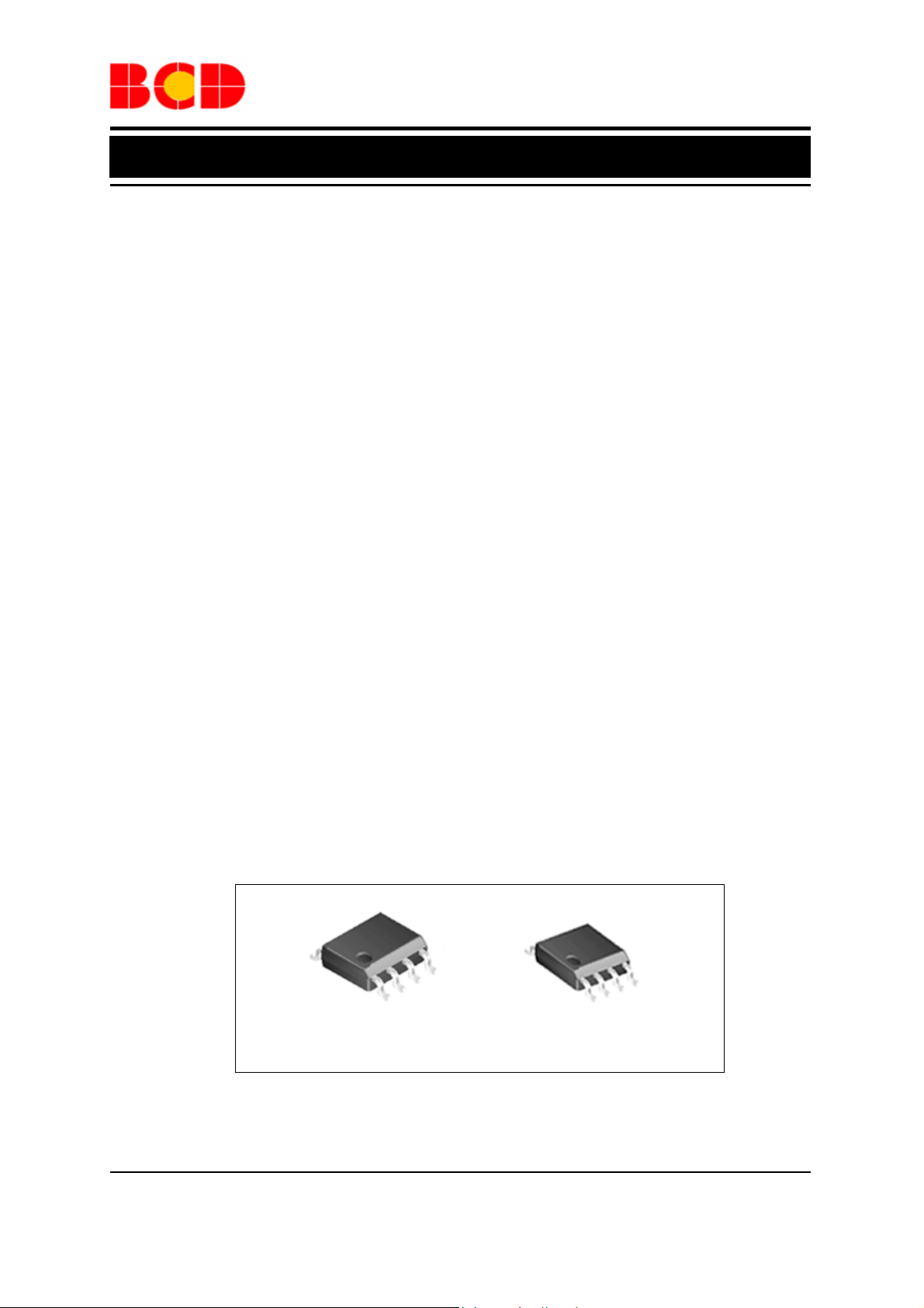
The AP2820 is available in standard packages of
SOIC-8 and MSOP-8.
, 60mΩ, is designed
DS(ON)
Applications
• USB Power Management
USB Bus/Self Powered Hubs
•
• Hot-plug Power Supplies
• Battery-charger Circuits
• Notebooks, Motherboard PCs
Features
•
Low MOSFET on Resistance: 60mΩ
• Compliant to USB Specifications
• Available 2 Versions of Load Ability:
Guarantee 2.0A Continuous Load for A/B/C/D
Version
Guarantee 2.5A Continuous Load for E/F/G/H
Version
• Logic Level Enable Pin: Available with
Active-high or Active-low Version
• Operating Voltage Range: 2.7V to 5.5V
• Low Supply Current:
75μA (Typ.) (For A/B/C/D versions)
80μA (Typ.) (For E/F/G/H versions)
• Low Shutdown Current: 1.0μA (Max)
• Under-voltage Lockout
• Soft Start-up
• Over-current Protection
• Over Temperature Protection
• Load Short Protection with Fold-back
• No Reverse Current When Power Off
• Deglitched FLAG Output with Open Drain
• With Output Shutdown Pull-low Resistor for
A/C/E/G Versions
• UL Approved (File No. E339337)
• Nemko CB Scheme IEC60950-1, Ref. Certif
No. NO62093
SOIC-8 MSOP-8
Figure 1. Package Types of AP2820
Jul. 2012 Rev 1. 7 BCD Semiconductor Manufacturing Limited
1
Page 2
Advance Datasheet
High-side Power Distribution Switch with Enable and Flag AP2820
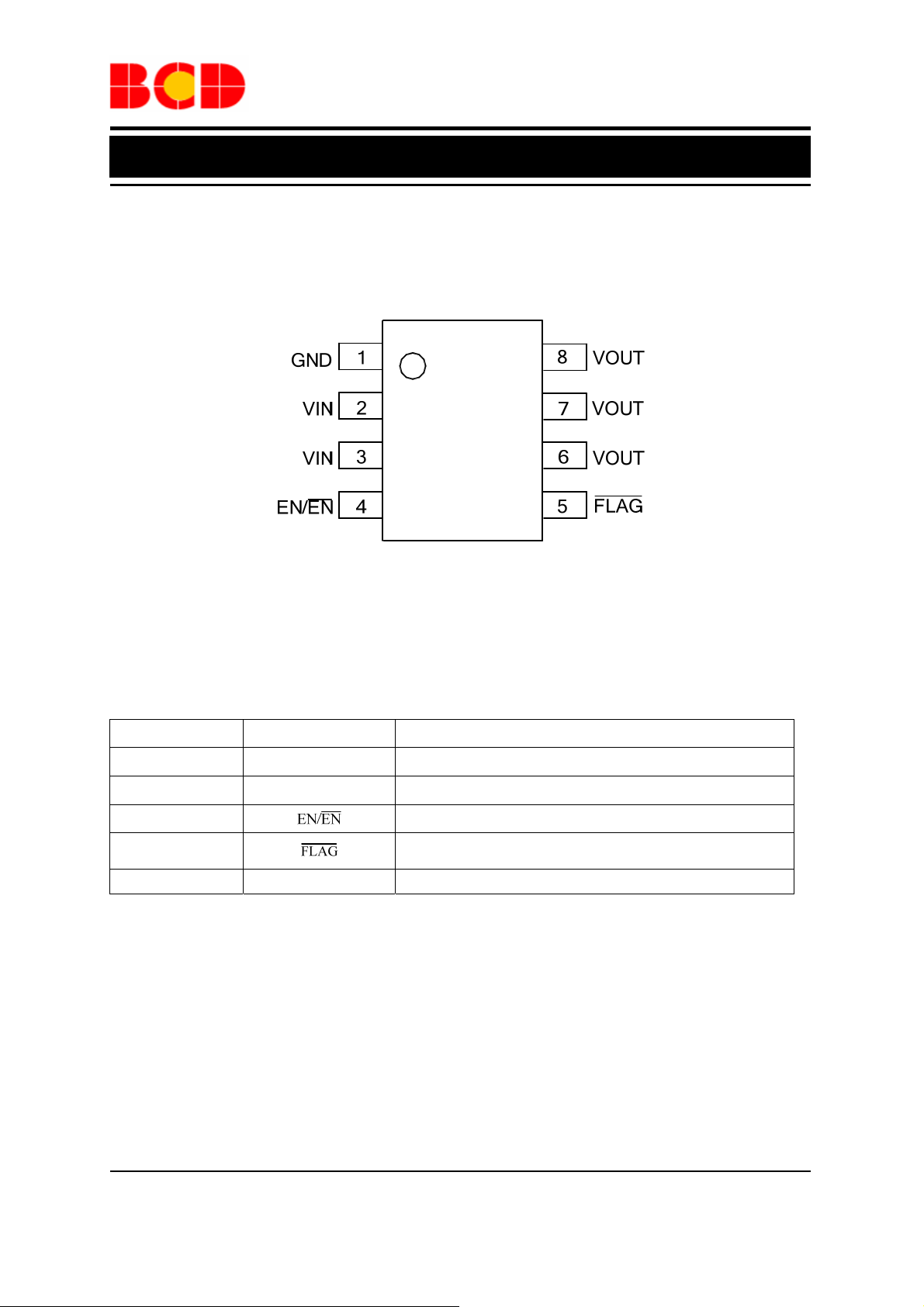
Pin Configuration
M/MM Package
(SOIC-8/MSOP-8)
Figure 2. Pin Configuration of AP2820 (Top View)
Pin Descriptions
Pin Number Pin Name Function
1 GND Ground
2, 3 VIN Supply input pin
4
5
6, 7, 8 VOUT Switch output voltage
Chip enable control input, active low or high
Fault flag pin, output with open drain, need a pull-up resistor
in application, active low to indicate OCP or OTP
Jul. 2012 Rev 1. 7 BCD Semiconductor Manufacturing Limited
2
Page 3
Advance Datasheet
High-side Power Distribution Switch with Enable and Flag AP2820
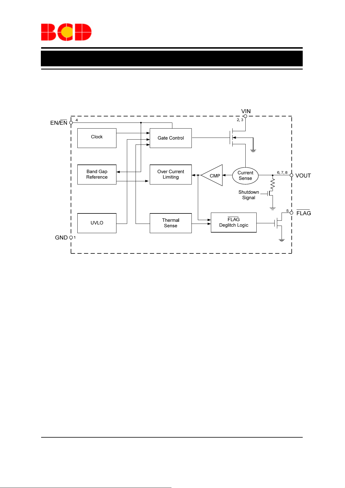
Functional Block Diagram
Figure 3. Functional Block Diagram of AP2820
Jul. 2012 Rev 1. 7 BCD Semiconductor Manufacturing Limited
3
Page 4
Advance Datasheet
High-side Power Distribution Switch with Enable and Flag AP2820
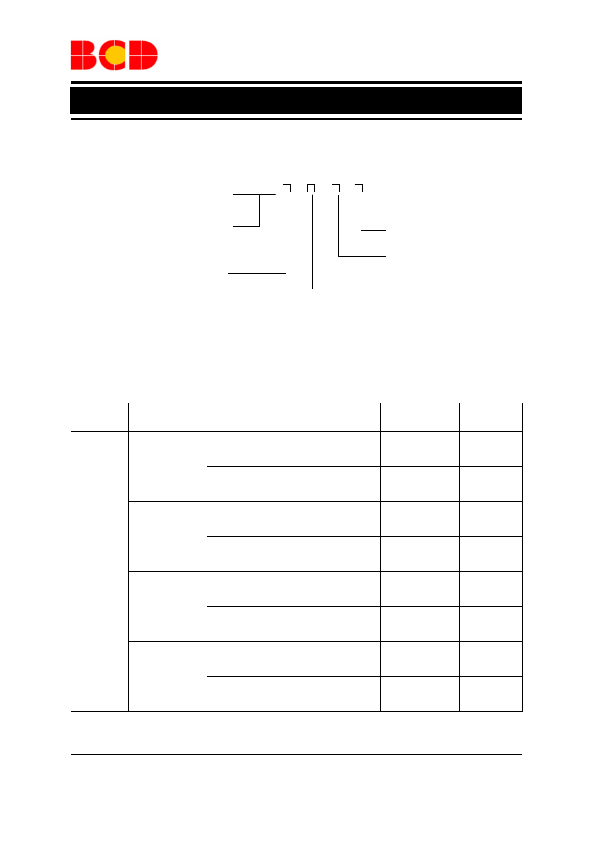
Ordering Information
AP2820 -
Circuit Type
Condition
For Continuous 2.0A Versions
A: Active High with Auto Discharge
B: Active High without Auto Discharge
C: Active Low with Auto Discharge
D: Active Low without Auto Discharge
For Continuous 2.5A Versions
E: Active High with Auto Discharge
F: Active High without Auto Discharge
G: Active Low with Auto Discharge
H: Active Low without Auto Discharge
Package
SOIC-8
Temperature
Range
-40 to 85°C
-40 to 85°C
-40 to 85°C
-40 to 85°C
Condition Part Number Marking ID
Active High
with Auto Discharge
(Continuous 2.0A)
Active High
without Auto Discharge
(Continuous 2.0A)
Active Low
with Auto Discharge
(Continuous 2.0A)
Active Low
without Auto Discharge
(Continuous 2.0A)
Active High
with Auto Discharge
(Continuous 2.5A)
Active High
without Auto Discharge
(Continuous 2.5A)
Active Low
with Auto Discharge
(Continuous 2.5A)
Active Low
without Auto Discharge
(Continuous 2.5A)
AP2820AM-G1 2820AM-G1 Tube
AP2820AMTR-G1 2820AM-G1 Tape & Reel
AP2820BM-G1 2820BM-G1 Tube
AP2820BMTR-G1 2820BM-G1 Tape & Reel
AP2820CM-G1 2820CM-G1 Tube
AP2820CMTR-G1 2820CM-G1 Tape & Reel
AP2820DM-G1 2820DM-G1 Tube
AP2820DMTR-G1 2820DM-G1 Tape & Reel
AP2820EM-G1 2820EM-G1 Tube
AP2820EMTR-G1 2820EM-G1 Tape & Reel
AP2820FM-G1 2820FM-G1 Tube
AP2820FMTR-G1 2820FM-G1 Tape & Reel
AP2820GM-G1 2820GM-G1 Tube
AP2820GMTR-G1 2820GM-G1 Tape & Reel
AP2820HM-G1 2820HM-G1 Tube
AP2820HMTR-G1 2820HM-G1 Tape & Reel
G1: Green
TR: Tape & Reel
Blank: Tube
Package
M: SOIC-8
MM: MSOP-8
Packing
Type
Jul. 2012 Rev 1. 7 BCD Semiconductor Manufacturing Limited
4
Page 5
Advance Datasheet
High-side Power Distribution Switch with Enable and Flag AP2820
Ordering Information (Continued)
Package
MSOP-8
Temperature
Range
-40 to 85°C
-40 to 85°C
-40 to 85°C
-40 to 85°C
Condition Part Number Marking ID
Active High
with Auto Discharge
(Continuous 2.0A)
Active High
without Auto Discharge
(Continuous 2.0A)
Active Low
with Auto Discharge
(Continuous 2.0A)
Active Low
without Auto Discharge
(Continuous 2.0A)
Active High
with Auto Discharge
(Continuous 2.5A)
Active High
without Auto Discharge
(Continuous 2.5A)
Active Low
with Auto Discharge
(Continuous 2.5A)
Active Low
without Auto Discharge
(Continuous 2.5A)
AP2820AMM-G1 2820AMM-G1 Tube
AP2820AMMTR-G1 2820AMM-G1 Tape & Reel
AP2820BMM-G1 2820BMM-G1 Tube
AP2820BMMTR-G1 2820BMM-G1 Tape & Reel
AP2820CMM-G1 2820CMM-G1 Tube
AP2820CMMTR-G1 2820CMM-G1 Tape & Reel
AP2820DMM-G1 2820DMM-G1 Tube
AP2820DMMTR-G1 2820DMM-G1 Tape & Reel
AP2820EMM-G1 2820EMM-G1 Tube
AP2820EMMTR-G1 2820EMM-G1 Tape & Reel
AP2820FMM-G1 2820FMM-G1 Tube
AP2820FMMTR-G1 2820FMM-G1 Tape & Reel
AP2820GMM-G1 2820GMM-G1 Tube
AP2820GMMTR-G1 2820GMM-G1 Tape & Reel
AP2820HMM-G1 2820HMM-G1 Tube
AP2820HMMTR-G1 2820HMM-G1 Tape & Reel
Packing
Type
BCD Semiconductor's Pb-free products, as designated with "G1" suffix in the part number, are RoHS compliant
and green.
Jul. 2012 Rev 1. 7 BCD Semiconductor Manufacturing Limited
5
Page 6
Advance Datasheet
High-side Power Distribution Switch with Enable and Flag AP2820
Absolute Maximum Ratings (Note 1)
Parameter Symbol Value Unit
Power Supply Voltage VIN 6.0 V
Operating Junction Temperature
Range
Storage Temperature Range T
Lead Temperature (Soldering, 10sec) T
150 ºC
T
J
-65 to 150 ºC
STG
260 ºC
LEAD
Thermal Resistance Junction to
Ambient
CDM (Charge Device Model)
ESD (Human Body Model) 2000 V
θ
JA
SOIC-8 135
MSOP-8 150
1000 V
o
C/W
Note 1: Stresses greater than those listed under “Absolute Maximum Ratings” may cause permanent damage to
the device. These are stress ratings only, and functional operation of the device at these or any other conditions
beyond those indicated under “Recommended Operating Conditions” is not implied. Exposure to “Absolute
Maximum Ratings” for extended periods may affect device reliability.
Recommended Operating Conditions
Parameter Symbol Min Max Unit
Supply Voltage VIN 2.7 5.5 V
Operating Ambient Temperature
Range
-40 85 °C
T
A
Jul. 2012 Rev 1. 7 BCD Semiconductor Manufacturing Limited
6
Page 7

t
Advance Datasheet
High-side Power Distribution Switch with Enable and Flag AP2820
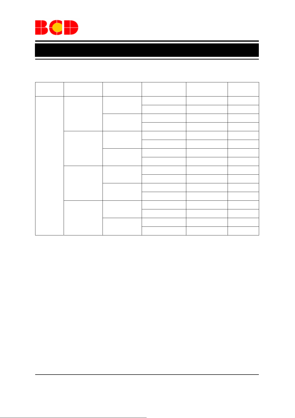
Electrical Characteristics
For A/B/C/D Versions
(VIN=5.0V, CIN=2.2μF, C
specified)
Parameter Symbol Condition Min Typ Max Unit
=1.0μF, Typical T
OUT
=25°C, Bold typeface applies over -40°C≤T
A
≤85°C ranges, unless otherwise
A
Input Voltage Range VIN
Switch On Resistance R
Current Limit I
Supply Current I
Fold-back Short Current I
Shutdown Supply Current I
Enable High Input Threshold V
Enable Low Input Threshold V
DS(ON)
LIMIT
SUPPLY
SHORT
SHUTDOWN
ENH
ENL
VIN=5V, I
V
OUT
=2.0A 60 80
OUT
=4.0V 2.2 2.7 3.2 A
VIN=5V, No Load 75 105
V
=0 1.18 A
OUT
Chip Disable, Shutdown Mode 0.1 1
1.6 5.5 V
0 1.0 V
2.7 5.5 V
Enable Pin Input Current IEN Force 0V to 5V at EN Pin -1.0 1.0
Under Voltage Lockou
Threshold Voltage
Under Voltage Hysteresis V
Reverse Current I
Output Pull Low Resistance
after Shutdown
R
Output Turn-on Time tON
FLAG Pin Delay Time t
FLAG Pin Low Voltage V
FLAG Pin Leakage Current I
Thermal Shutdown
Temperature
Thermal Shutdown Hysteresis T
VIN Increasing from 0V 2.2 2.5 2.7 V
V
UVLO
0.2 V
UVLOHY
Chip Disable, V
REVERSE
DISCHARGE
AP2820A, AP2820C Only 100 200
From Enable Active to 90% of
Output
From Over Current Fault
DFLG
FLG
LEAKAGE
T
OTSD
HYOTSD
Condition to Flag Active
I
=5mA 35 70 mV
SINK
FLAG Disable, Force 5.0V 1.0
0.1 1.0
OUT>VIN
500
5 10 15 ms
150 °C
30 °C
mΩ
μA
μA
μA
μA
Ω
μs
μA
Jul. 2012 Rev 1. 7 BCD Semiconductor Manufacturing Limited
7
Page 8

t
Advance Datasheet
High-side Power Distribution Switch with Enable and Flag AP2820
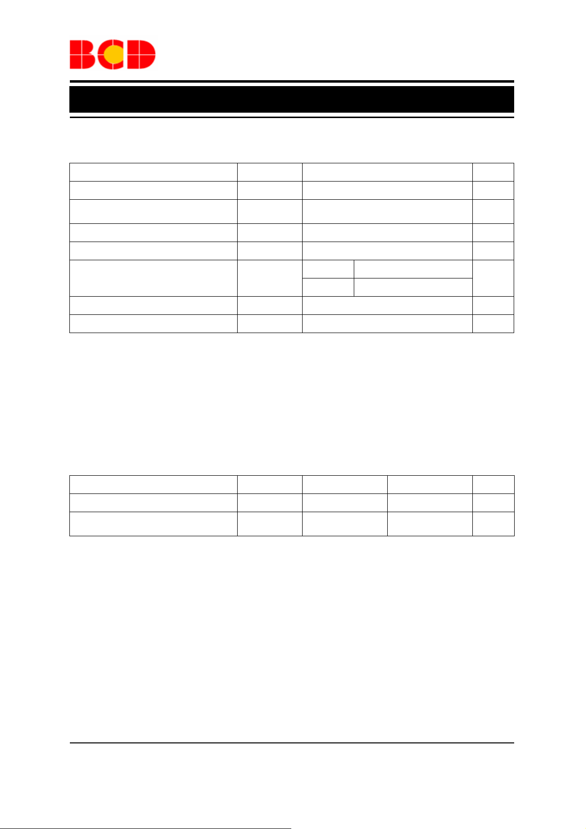
Electrical Characteristics (Continued)
For E/F/G/H Versions
(VIN=5.0V, CIN=2.2μF, C
specified)
Parameter Symbol Condition Min Typ Max Unit
=1.0μF, Typical T
OUT
=25°C, Bold typeface applies over -40°C≤T
A
≤85°C ranges, unless otherwise
A
Input Voltage Range VIN
Switch On Resistance R
Current Limit I
Supply Current I
Fold-back Short Current I
Shutdown Supply Current I
Enable High Input Threshold V
Enable Low Input Threshold V
DS(ON)
LIMIT
SUPPLY
SHORT
SHUTDOWN
ENH
ENL
VIN=5V, I
V
OUT
=2.5A 60 80
OUT
=4.0V 2.8 3.4 4.2 A
VIN=5V, No Load 80 110
V
=0 1.18 A
OUT
Chip Disable, Shutdown Mode 0.1 1
1.6 5.5 V
0 1.0 V
2.7 5.5 V
Enable Pin Input Current IEN Force 0V to 5V at EN Pin -1.0 1.0
Under Voltage Lockou
Threshold Voltage
Under Voltage Hysteresis V
Reverse Current I
Output Pull Low Resistance
after Shutdown
R
Output Turn-on Time tON
FLAG Pin Delay Time t
FLAG Pin Low Voltage V
FLAG Pin Leakage Current I
Thermal Shutdown
Temperature
Thermal Shutdown Hysteresis T
VIN Increasing from 0V 2.2 2.5 2.7 V
V
UVLO
0.2 V
UVLOHY
Chip Disable, V
REVERSE
DISCHARGE
AP2820E, AP2820G Only 100 200
From Enable Active to 90% of
Output
From Over Current Fault
DFLG
FLG
LEAKAGE
T
OTSD
HYOTSD
Condition to Flag Active
I
=5mA 35 70 mV
SINK
FLAG Disable, Force 5.0V 1.0
0.1 1.0
OUT>VIN
500
5 10 15 ms
150
30
mΩ
μA
μA
μA
μA
Ω
μs
μA
o
C
o
C
Jul. 2012 Rev 1. 7 BCD Semiconductor Manufacturing Limited
8
Page 9

Advance Datasheet
High-side Power Distribution Switch with Enable and Flag AP2820
Typical Performance Characteristics
100
90
80
70
60
50
40
30
Supply Current (μA)
20
10
0
-40.0 -20.0 0.0 20.0 40.0 60.0 80.0
Ambient Temperature (
For AP2820A/B/C/D Versions
O
C)
VIN=5V
Enable Active
No Load
Figure 4. Supply Current vs. Ambient Temperature Figure 5. Supply Current vs. Ambient Temperature
100
90
80
70
60
50
40
30
Supply Current (μA)
20
10
0
-10
1.0 1.5 2.0 2.5 3.0 3.5 4.0 4.5 5.0 5.5
Supply Voltage (V)
TA=-40OC
TA=25OC
TA=85OC
For AP2820A/B/C/D Versions
TA=25OC
Enable Active
Figure 6. Supply Current vs. Supply Voltage Figure 7. Current Limit vs. Supply Voltage
100
90
80
70
60
50
40
Supply Current (μA)
30
20
10
0
-40.0 -20.0 0.0 20.0 40.0 60.0 80.0
3.0
2.8
2.6
2.4
Current Limit (A)
2.2
2.0
3.0 3.5 4.0 4.5 5.0 5.5
Ambient Temperature (OC)
Supply Voltage (V)
For AP2820E/F/G/H Versions
TA=25OC
For AP2820A/B/C/D Versions
VIN=5V
Enable Active
No Load
VIN=5V
Enable Active
Jul. 2012 Rev 1. 7 BCD Semiconductor Manufacturing Limited
9
Page 10

Advance Datasheet
High-side Power Distribution Switch with Enable and Flag AP2820
Typical Performance Characteristics (Continued)
3.2
3.1
3.0
2.9
2.8
2.7
2.6
2.5
Current Limit (A)
2.4
2.3
2.2
2.1
2.0
-40.0 -20.0 0.0 20.0 40.0 60.0 80.0
Ambient Temperature (OC)
For AP2820A/B/C/D Versions
VIN=5V
Enable Active
3.4
3.2
3.0
Current Limit (A)
2.8
2.6
-40.0 -20.0 0.0 20.0 40.0 60.0 80.0
Ambient Temperature (
For AP2820E/F/G/H Versions
Figure 8. Current Limit vs. Ambient Temperature Figure 9. Current Limit vs. Ambient Temperature
100
90
80
70
60
50
40
30
Switch On Resistance (mΩ)
20
10
0
-40.0 -20.0 0.0 20.0 40.0 60.0 80.0
I
=2.0A
OUT
For AP2820A/B/C/D Versions
Ambient Temperature (OC)
VIN=5V
Enable Active
100
90
80
70
60
50
40
30
Switch On Resistance (mΩ)
20
10
0
-40.0 -20.0 0.0 20.0 40.0 60.0 80.0
I
=2.5A
OUT
For AP2820E/F/G/H Vers ions
Ambient Temperature (OC)
Figure 10. Switch On Resistance Figure 11. Switch On Resistance
vs. Ambient Temperature vs. Ambient Temperature
VIN=5V
Enable Active
O
C)
VIN=5V
Enable Active
Jul. 2012 Rev 1. 7 BCD Semiconductor Manufacturing Limited
10
Page 11

Advance Datasheet
High-side Power Distribution Switch with Enable and Flag AP2820
Typical Performance Characteristics (Continued)
100
90
I
=2.0A
OUT
Enable Active
80
70
60
50
Switch On Resistance (mΩ)
40
30
3.0 3.5 4.0 4.5 5.0 5.5
TA=25OC
Supply Voltage (V)
Figure 12. Switch On Resistance vs. Supply Voltage Figure 13. UVLO Voltage vs. Ambient Temperature
15
14
13
12
11
10
9
8
7
6
Flag Delay Time during Over Current (mS)
5
-40.0 -20.0 0.0 20.0 40.0 60.0 80.0
Ambient Temperature (OC)
VIN=5V
Enable Active
Figure 14. Flag Delay Time during Over Current Figure 15. Flag Delay Time during Over Current
vs. Ambient Temperature vs. Supply Voltage
2.70
2.65
2.60
2.55
2.50
2.45
2.40
2.35
2.30
2.25
2.20
Under Voltage Lockout Threshold Voltage (V)
-40.0 -20.0 0.0 20.0 40.0 60.0 80.0
14
12
10
8
6
Flag Delay Time during Over Current (mS)
3.0 3.5 4.0 4.5 5.0 5.5
VIN Rising
VIN Falling
Ambient Temperature (
TA=25OC
Supply Voltage (V)
Enable Active
O
C)
VIN=5V
Enable Active
Jul. 2012 Rev 1. 7 BCD Semiconductor Manufacturing Limited
11
Page 12

Advance Datasheet
High-side Power Distribution Switch with Enable and Flag AP2820
Typical Performance Characteristics (Continued)
1.30
1.28
1.26
1.24
1.22
1.20
1.18
1.16
1.14
1.12
1.10
1.08
1.06
Output Short to GND Current (A)
1.04
1.02
1.00
3.0 3.5 4.0 4.5 5.0
Supply Voltage (V)
Figure 16. Output Short to GND Current Figure 17. Output Short to GND Current
vs. Supply Voltage vs. Ambient Temperature
1.6
1.5
1.4
1.3
V
EN_H
VIN=5V
1.2
1.1
Enable Threshold Voltage (V)
1.0
-40.0 -20.0 0.0 20.0 40.0 60.0 80.0
V
EN_L
Ambient Temperature (OC)
Figure 18. Enable Threshold Voltage Figure 19. Enable Threshold Voltage
vs. Ambient Temperature vs. Supply Voltage
VIN=5V
Enable Active
1.5
1.4
1.3
1.2
1.1
Output Short to GND Current (A)
1.0
-40.0 -20.0 0.0 20.0 40.0 60.0 80.0
Ambient Temperature (OC)
1.7
1.6
1.5
1.4
1.3
1.2
1.1
1.0
0.9
Enable Threshold Voltage (V)
0.8
0.7
3.0 3.5 4.0 4.5 5.0 5.5
V
EN_H
Supply Voltage (V)
V
VIN=5V
Enable Active
EN_L
TA=25OC
Jul. 2012 Rev 1. 7 BCD Semiconductor Manufacturing Limited
12
Page 13

v
Advance Datasheet
High-side Power Distribution Switch with Enable and Flag AP2820
Typical Performance Characteristics (Continued)
5V/div
I
20mA/div
1V/div
5V/div
1V/div
I
1A/div
VEN
INRUSH
V
OUT
Time 5 00μs/div
Figure 20. Output Turn On and Rise Time
(CIN=1.0μF, C
=1.0μF, No Load) (CIN=1.0μF, C
OUT
VEN
V
OUT
INRUSH
Time 5 00μs/div
Figure 22. Output Turn On and Rise Time Figure 23. Output Turn Off and Fall Time
(C
=1.0μF, C
IN
=220μF, No Load) (VIN=5V, CIN=1.0μF, No Load)
OUT
V
5V/div
I
INRUSH
1A/div
V
OUT
1V/div
V
5V/di
V
OUT
1V/div
EN
Time 5 00μs/div
Figure 21. Output Turn On and Rise Time
=1.0μF, RL=3.3Ω)
OUT
EN
=470μF
C
OUT
=100μF
C
OUT
=22μF
C
OUT
C
=1μF
OUT
Time 5ms/div
C
OUT
=220μF
Jul. 2012 Rev 1. 7 BCD Semiconductor Manufacturing Limited
13
Page 14

Advance Datasheet
High-side Power Distribution Switch with Enable and Flag AP2820
Typical Performance Characteristics (Continued)
VEN
5V/div
V
OUT
1V/div
I
OUT
1A/div
Time 5 00μs/div
Figure 24. Output Turn Off and Fall Time
(VIN=5V, CIN=1.0μF, C
=470μF, RL=3.3Ω) (VIN=5V, CIN=1.0μF)
OUT
V
FLAG
1V/div
I
OUT
1A/div
V
OUT
1V/div
Time 5ms/div
Figure 26. FLAG Response during Over Current Figure 27. FLAG Response during
Over Temperature (T
V
EN
5V/div
I
OUT
1A/div
V
OUT
1V/div
Time 20ms/div
Figure 25. Output Short to GND Current
V
FLAG
1V/div
I
OUT
1A/div
V
OUT
1V/div
Time 5ms/div
=125oC)
A
Jul. 2012 Rev 1. 7 BCD Semiconductor Manufacturing Limited
14
Page 15

Advance Datasheet
High-side Power Distribution Switch with Enable and Flag AP2820
Typical Application
Note 2: 2.2μF input capacitor is enough in most application cases.
If the VOUT is short to ground frequently during usage, large size input capacitor is necessary, recommend
22μF.
Figure 28. Typical Application of AP2820
Jul. 2012 Rev 1. 7 BCD Semiconductor Manufacturing Limited
15
Page 16

Advance Datasheet
High-side Power Distribution Switch with Enable and Flag AP2820
Mechanical Dimensions
SOIC-8 Unit: mm(inch)
R0.150(0.006)
Jul. 2012 Rev 1. 7 BCD Semiconductor Manufacturing Limited
16
Page 17

Advance Datasheet
High-side Power Distribution Switch with Enable and Flag AP2820
Mechanical Dimensions (Continued)
MSOP-8 Unit: mm(inch)
)
)
4
2
1
2
1
1
.
.
0
0
(
(
0
0
0
0.410(0.016)
0.650(0.026)
4.700(0.185)
5.100(0.201)
0
9
1
.
.
2
3
)
)
0
8
0
0
0
0
.
.
0
0
(
(
0
0
0
0
0
2
.
.
0
0
Jul. 2012 Rev 1. 7 BCD Semiconductor Manufacturing Limited
17
Page 18

BCD Semiconductor Manufacturing Limited
IMPORTANT NOTICE
IMPORTANT NOTICE
BCD Semiconductor Manufacturing Limited reserves the right to make changes without further notice to any products or specifi-
BCD Semiconductor Manufacturing Limited reserves the right to make changes without further notice to any products or specifi-
cations herein. BCD Semiconductor Manufacturing Limited does not assume any responsibility for use of any its products for any
cations herein. BCD Semiconductor Manufacturing Limited does not assume any responsibility for use of any its products for any
particular purpose, nor does BCD Semiconductor Manufacturing Limited assume any liability arising out of the application or use
particular purpose, nor does BCD Semiconductor Manufacturing Limited assume any liability arising out of the application or use
of any its products or circuits. BCD Semiconductor Manufacturing Limited does not convey any license under its patent rights or
of any its products or circuits. BCD Semiconductor Manufacturing Limited does not convey any license under its patent rights or
other rights nor the rights of others.
other rights nor the rights of others.
http://www.bcdsemi.com
MAIN SITE
MAIN SITE
- Headquarters
BCD Semiconductor Manufacturing Limited
BCD Semiconductor Manufactur ing Limited
- Wafer Fab
No. 1600, Zi Xing Road, Shanghai ZiZhu Science-based Industrial Park, 200241, China
Shanghai SIM-BCD Semiconductor Manufacturing Limited
Tel: +86-21-24162266, Fax: +86-21-24162277
800, Yi Shan Road, Shanghai 200233, China
Tel: +86-21-6485 1491, Fax: +86-21-5450 0008
REGIONAL SALES OFFICE
Shenzhen Office
REGIONAL SALES OFFICE
Shanghai SIM-BCD Semiconductor Manufacturing Co., Ltd., Shenzhen Office
Shenzhen Office
Unit A Room 1203, Skyworth Bldg., Gaoxin Ave.1.S., Nanshan District, Shenzhen,
Shanghai SIM-BCD Semiconductor Manufacturing Co., Ltd. Shenzhen Office
China
Advanced Analog Circuits (Shanghai) Corporation Shenzhen Office
Tel: +86-755-8826 7951
Room E, 5F, Noble Center, No.1006, 3rd Fuzhong Road, Futian District, Shenzhen 518026, China
Fax: +86-755-8826 7865
Tel: +86-755-8826 7951
Fax: +86-755-8826 7865
- Wafer Fab
BCD Semiconductor Manufacturing Limited
Shanghai SIM-BCD Semiconductor Manufacturing Co., Ltd.
- IC Design Group
800 Yi Shan Road, Shanghai 200233, China
Advanced Analog Circuits (Shanghai) Corporation
Tel: +86-21-6485 1491, Fax: +86-21-5450 0008
8F, Zone B, 900, Yi Shan Road, Shanghai 200233, China
Tel: +86-21-6495 9539, Fax: +86-21-6485 9673
Taiwan Office
BCD Semiconductor (Taiwan) Company Limited
Taiwan Office
4F, 298-1, Rui Guang Road, Nei-Hu District, Taipei,
BCD Semiconductor (Taiwan) Company Limited
Tai wan
4F, 298-1, Rui Guang Road, Nei-Hu District, Taipei,
Tel: +886-2-2656 2808
Taiwan
Fax: +886-2-2656 2806
Tel: +886-2-2656 2808
Fax: +886-2-2656 2806
USA Office
BCD Semiconductor Corp.
USA Office
30920 Huntwood Ave. Hayward,
BCD Semiconductor Corporation
CA 94544, USA
30920 Huntwood Ave. Hayward,
Tel : +1-510-324-2988
CA 94544, U.S.A
Fax: +1-510-324-2788
Tel : +1-510-324-2988
Fax: +1-510-324-2788
 Loading...