

Page 1
4-CH Linear Constant Current Sink With Matching AP2502
Data Sheet
General Description
The AP2502 is a 4-channel independent linear
current sink with low dropout voltage and perfect
match between each channel. Each channel can
provide 20mA continuous constant current.
In application, there is only one 0.1µF ceramic
capacitor required, and there is no any EMI and
switching noise issue. It is perfect choice for
hand-hold portable system especially based on
Li-ion/Polymer battery power e d di spl ay module.
The brightness can be controlled and/or adjustable
via simple PWM signal applied to EN pin.
The AP2502 is available with SOT-23-6 and
TSOT-23-6 packages.
Features
• Current Matching Between Each Channel: ±1%
• Low Dropout Voltage: 65mV (Typ.) @ I
20mA
• Maximum Output Current on Each Channel:
20mA
• Ultra-low Quiescent Current: 125µA (Typ.)
• Ultra-low Shutdown Current: 1µA (Max.)
• None EMI and Switching Noise Issue
• Permitted PWM Dimming Frequency up to
• 150kHz
• OTSD Protection
LED
Applications
• Mobile Phone, Smart Phone, PDA
• MP3, MP4, PMP
• Small Size Backlight Module
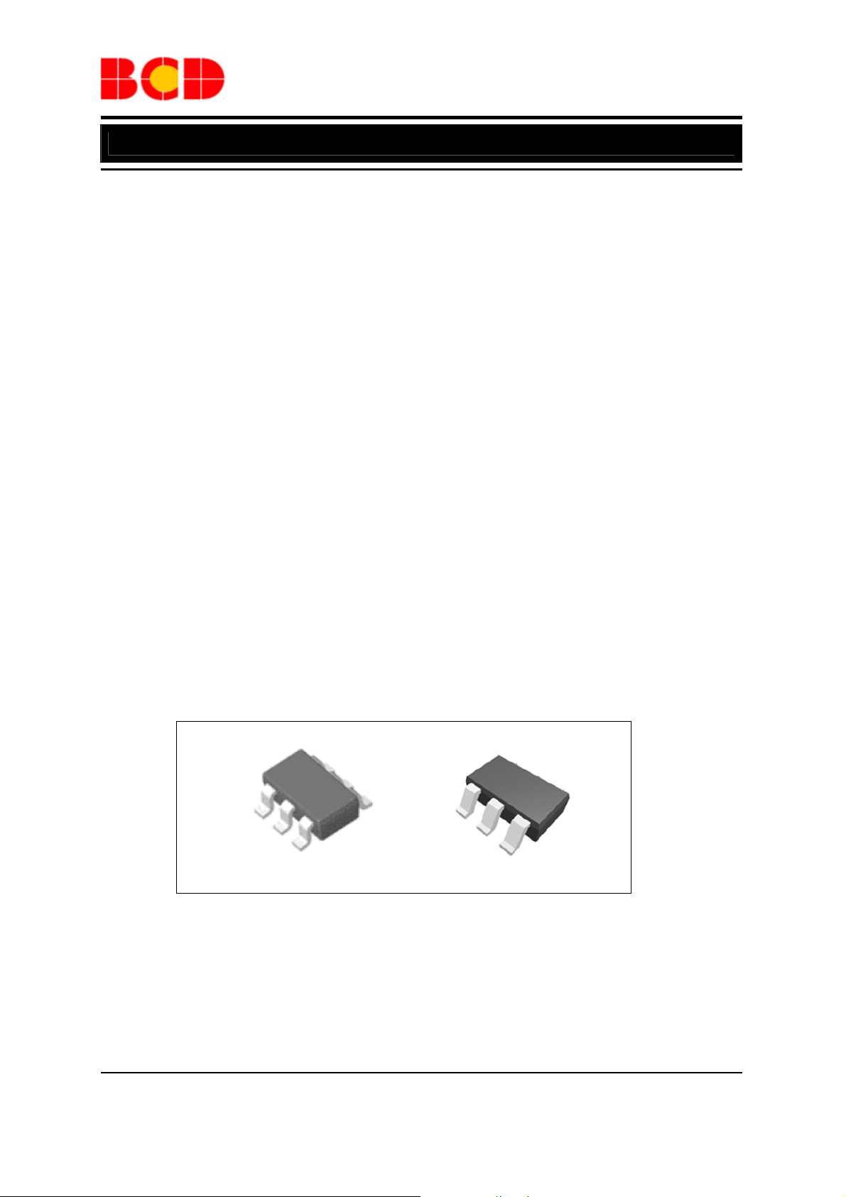
SOT-23-6 TSOT-23-6
Figure 1. Package Types of AP2502
=
Oct. 2010 Rev 1. 1 BCD Semiconductor Manufacturing Limited
1
Page 2
Data Sheet
4-CH Linear Constant Current Sink With Matching AP2502
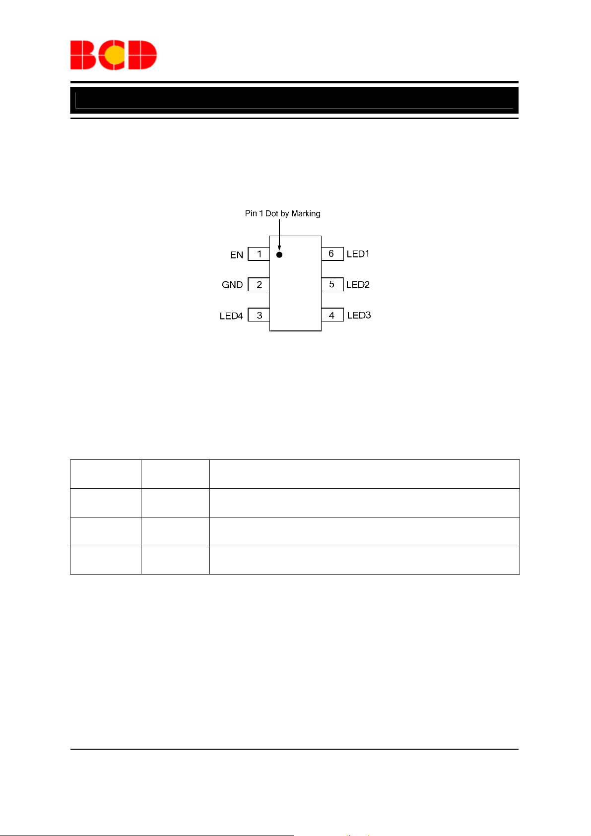
Pin Configuration
K/KT Package
(SOT-23-6/TSOT-23-6)
Figure 2. Pin Configuration of AP2502 (Top View)
Pin Descriptions
P in Number Pin Name Description
1 EN
2 GND GND
3, 4, 5, 6 LED4 to LED1 LED cathode terminal for channel number
Oct. 2010 Rev 1. 1 BCD Semiconductor Manufacturing Limited
Chip enable pin, active high to permit PWM signal input for brightness control by
changing duty cycle
2
Page 3
Data Sheet
4-CH Linear Constant Current Sink With Matching AP2502
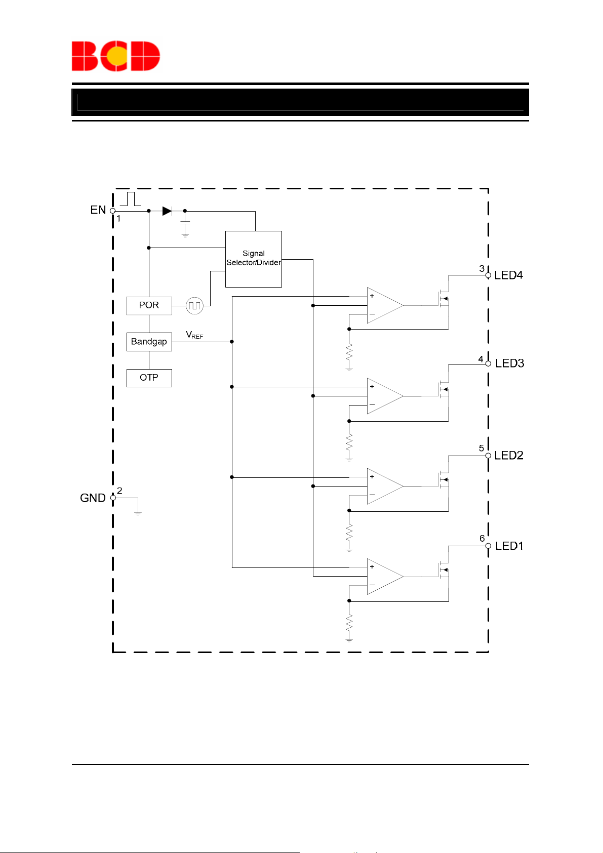
Functional Block Diagram
Figure 3. Functional Block Diagram of AP2502
Oct. 2010 Rev 1. 1 BCD Semiconductor Manufacturing Limited
3
Page 4
Data Sheet
4-CH Linear Constant Current Sink With Matching AP2502
Ordering Information
AP2502 -
Circuit Type G1: Green
Package
K: SOT-23-6
KT: TSOT-23-6
Package
SOT-23-6
TSOT-23-6
BCD Semiconductor's Pb-free products, as designated with "G1" suffix in the part number, are RoHS compliant
and Green.
Temperature
Range
-40 to 85°C
-40 to 85°C
Part Number Marking ID
AP2502KTR-G1 GEE Tape & Reel
AP2502KTTR-G1 L7E Tape & Reel
TR: Tape & Reel
Packing
Type
Absolute Maximum Ratings (Note 1)
Parameter Symbol Value Unit
Enable Input Voltage VEN -0.3 to 6.5 V
Thermal Resistance (Junction to Ambient)
Operating Junction Temperature Range TJ 150 ºC
Storage Temperature Range T
Lead Temperature (Soldering,10 seconds) T
ESD (Machine Model) 600 V
ESD (Human Body Model) 6000 V
θ
JA
-65 to 150 ºC
STG
260 ºC
LEAD
250 ºC/W
Note 1: Stresses greater than those listed under “Absolute Maximum Ratings” may cause permanent damage to
the device. These are stress ratings only, and functional operation of the device at these or any other conditions
beyond those indicated under “Recommended Operating Conditions” is not implied. Exposure to “Absolute
Maximum Ratings” for extended periods may affect device reliability.
Oct. 2010 Rev 1. 1 BCD Semiconductor Manufacturing Limited
4
Page 5

k
Data Sheet
4-CH Linear Constant Current Sink With Matching AP2502
Recommended Operating Conditions
Parameter Symbol
Unit
Min Max
Value
Enable Input Voltage VEN 2.0 6.0 V
Operating Temperature Range TA -40 85 °C
Sink Current I
20 mA
LED
Electrical Characteristics
VIN=3.6V, V
Parameter Symbol Test Conditions Min Typ Max Unit
LED Dropout Voltage V
Enable PIN High Voltage VIH 2 6 V
=3.2V, TA = 25°C, unless otherwise specified.
F_LED
DROPOUT
I
=20mA 65 120 mV
SINK
Enable PIN Low Voltage VIL 0 0.5 V
LED Maximum Sin
Current
Sink Current Matching
Between each Chann el
I
LED(MAX)
I
LED-MATCH
Quiescent Current IQ I
Shutdown Current I
SHUTDOWN
Thermal Resistance (Junction
to Case)
PWM Frequency to Adjust
Brightness
EN Pin Pulse High Time T
EN Pin Pulse Low Time T
Thermal Shutdown
Temperature
Thermal Shutdown
Hysteresis
Oct. 2010 Rev 1. 1 BCD Semiconductor Manufacturing Limited
T
T
VCC=3.3 to 6.0V, Enable=VCC 18 20 22 mA
V
Set EN Pin Low 0.1 1
θ
JC
150 kHz
f
PWM
1
HIGH
100 ns
LOW
150
OTSD
=0.4V 0.5 1 %
LED
LED1=ILED2=ILED3=ILED4
=20mA 125 180
µA
µA
80
°C/W
µs
°C
25
HYOTSD
5
Page 6

Data Sheet
4-CH Linear Constant Current Sink With Matching AP2502
Typical Performance Characteristics
200
190
180
Quiescent Current (µA)
LED Open
170
V
=3V
160
150
140
130
120
110
100
EN
90
80
70
60
50
-40 -20 0 20 40 60 80 100 120 140
Case Temperature (oC)
Figure 4. Quiescent Current vs. Case Temperature Figure 5. Quiescent Current vs. Enable Voltage
21.0
20.8
20.6
20.4
20.2
20.0
(mA)
19.8
LED
I
19.6
19.4
19.2
19.0
VEN=3V
=4V
V
IN
-40-200 20406080100120
Case Temperature (OC)
Figure 6. LED Current vs. Case Temperature Figure 7. LED Current vs. Output Voltage
Oct. 2010 Rev 1. 1 BCD Semiconductor Manufacturing Limited
200
190
LED Open
180
170
160
150
140
130
120
110
100
90
Quiescent Current (µA)
80
70
60
22
20
18
16
14
12
10
(mA)
LED
I
8
6
4
2
0
TC=-40oC
TC=25oC
TC=85oC
1234567
Enable Voltage (V)
VEN=3V
TC=-40oC
TC=25oC
TC=85oC
0 100 200 300 400 500 600 700 800 900 1000
Output Voltage (mV)
6
Page 7

Data Sheet
4-CH Linear Constant Current Sink With Matching AP2502
Typical Performance Characteristics (Continued)
120
110
100
90
80
70
60
50
Dropout Voltage (mV)
40
30
20
-40 -20 0 20 40 60 80 100 120 140
Case Temperature (oC)
Figure 8. Dropout Voltage vs. Case Temperature Figure 9. Current Matching vs. Case Temperature
24.0
23.5
23.0
22.5
22.0
21.5
21.0
20.5
20.0
(mA)
19.5
LED
I
19.0
18.5
18.0
17.5
17.0
16.5
16.0
2.0 2.5 3.0 3.5 4.0 4.5 5.0 5.5 6.0
Enable Voltage (V)
V
=300mV
LED
TC=25oC
Figure 10. LED Current vs. Enable Voltage Figure 11. LED Current Efficiency vs. Duty Cycle
1.0
0.8
0.6
0.4
0.2
0.0
-0.2
-0.4
Current Matching (%)
-0.6
-0.8
-1.0
-40 -20 0 20 40 60 80 100 120 140
Case Temperature (oC)
110
100
90
80
70
60
50
40
30
20
LED Current Efficiency (%)
10
0
-10
0 102030405060708090
Duty Cycle (%)
T
C
VEN=3V
V
=25oC
=300mV
LED
f=100Hz
f=10kHz
f=100kHz
f=150kHz
99
Oct. 2010 Rev 1. 1 BCD Semiconductor Manufacturing Limited
7
Page 8

Data Sheet
4-CH Linear Constant Current Sink With Matching AP2502
Typical Performance Characteristics (Continued)
VEN
2V/div
10mA/div
I
LED
I1 I
2
2V/div
10mA/div
V
I
EN
LED
Time 400µs/div
Time 2ms/div
Figure 12. LED Current (Note 2) Figure 13. Internal Oscillator Working at Low Frequency
(VIN=4V, VEN=0 to 3.6V, Duty cycle=50%, f
Note 2: Chopper offset-canceling technology is adopted to ge t good current matching, I
=1kHz) (VIN=4V, VEN=0 to 3.6V, Duty cycle=50%, f
PWM
=[(I1+I2)/2]*duty.
LED
=0.1kHz)
PWM
Oct. 2010 Rev 1. 1 BCD Semiconductor Manufacturing Limited
8
Page 9

Data Sheet
4-CH Linear Constant Current Sink With Matching AP2502
Typical Application
Figure 14. AP2502 Typical Application
Oct. 2010 Rev 1. 1 BCD Semiconductor Manufacturing Limited
9
Page 10

Data Sheet
4-CH Linear Constant Current Sink With Matching AP2502
Mechanical Dimensions
SOT-23-6 Unit: mm(inch)
0°
8°
0.200(0.008)
0.300(0.012)
0.400(0.016)
6
2.820(0.111)
3.020(0.119)
5
0.300(0.012)
0.600(0.024)
4
Pin 1 Dot by Marking
123
0.950(0.037)TYP
1.800(0.071)
2.000(0.079)
0.700(0.028)REF
0.000(0.000)
0.150(0.006)
0.900(0.035)
1.300(0.051)
0.100(0.004)
0.200(0.008)
1.450(0.057)
MAX
Oct. 2010 Rev 1. 1 BCD Semiconductor Manufacturing Limited
10
Page 11

Data Sheet
4-CH Linear Constant Current Sink With Matching AP2502
Mechanical Dimensions (Continued)
TSOT-23-6 Unit: mm(inch)
°
2.800(0.110)
3.000(0.118)
R0.100(0.004)
MIN
0
8
°
1.500(0.059)
1.700(0.067)
0.950(0.037)
BSC
0.000(0.000)
0.100(0.004)
0.700(0.028)
0.900(0.035)
Pin 1 Dot by
Marking
1.900(0.075)
BSC
0.350(0.014)
0.510(0.020)
2.600(0.102)
3.000(0.118)
1.000(0.039)
MAX
GAUGE
PLANE
0.370(0.015)
MIN
0.100(0.004)
0.250(0.010)
0.250(0.010)
BSC
Oct. 2010 Rev 1. 1 BCD Semiconductor Manufacturing Limited
11
Page 12

BCD Semiconductor Manufacturing Limited
IMPORTANT NOTICE
IMPORTANT NOTICE
BCD Semiconductor Manufacturing Limited reserves the right to make changes without further notice to any products or specifi-
BCD Semiconductor Manufacturing Limited reserves the right to make changes without further notice to any products or specifi-
cations herein. BCD Semiconductor Manufacturing Limited does not assume any responsibility for use of any its products for any
cations herein. BCD Semiconductor Manufacturing Limited does not assume any responsibility for use of any its products for any
particular purpose, nor does BCD Semiconductor Manufacturing Limited assume any liability arising out of the application or use
particular purpose, nor does BCD Semiconductor Manufacturing Limited assume any liability arising out of the application or use
of any its products or circuits. BCD Semiconductor Manufacturing Limited does not convey any license under its patent rights or
of any its products or circuits. BCD Semiconductor Manufacturing Limited does not convey any license under its patent rights or
other rights nor the rights of others.
other rights nor the rights of others.
http://www.bcdsemi.com
MAIN SITE
MAIN SITE
- Headquarters
BCD Semiconductor Manufacturing Limited
BCD Semiconductor Manufactur ing Limited
- Wafer Fab
No. 1600, Zi Xing Road, Shanghai ZiZhu Science-based Industrial Park, 200241, China
Shanghai SIM-BCD Semiconductor Manufacturing Limited
Tel: +86-21-24162266, Fax: +86-21-24162277
800, Yi Shan Road, Shanghai 200233, China
Tel: +86-21-6485 1491, Fax: +86-21-5450 0008
REGIONAL SALES OFFICE
Shenzhen Office
REGIONAL SALES OFFICE
Shanghai SIM-BCD Semiconductor Manufacturing Co., Ltd., Shenzhen Office
Shenzhen Office
Unit A Room 1203, Skyworth Bldg., Gaoxin Ave.1.S., Nanshan District, Shenzhen,
Shanghai SIM-BCD Semiconductor Manufacturing Co., Ltd. Shenzhen Office
China
Advanced Analog Circuits (Shanghai) Corporation Shenzhen Office
Tel: +86-755-8826 7951
Room E, 5F, Noble Center, No.1006, 3rd Fuzhong Road, Futian District, Shenzhen 518026, China
Fax: +86-755-8826 7865
Tel: +86-755-8826 7951
Fax: +86-755-8826 7865
- Wafer Fab
BCD Semiconductor Manufacturing Limited
Shanghai SIM-BCD Semiconductor Manufacturing Co., Ltd.
- IC Design Group
800 Yi Shan Road, Shanghai 200233, China
Advanced Analog Circuits (Shanghai) Corporation
Tel: +86-21-6485 1491, Fax: +86-21-5450 0008
8F, Zone B, 900, Yi Shan Road, Shanghai 200233, China
Tel: +86-21-6495 9539, Fax: +86-21-6485 9673
Taiwan Office
BCD Semiconductor (Taiwan) Company Limited
Taiwan Office
4F, 298-1, Rui Guang Road, Nei-Hu District, Taipei,
BCD Semiconductor (Taiwan) Company Limited
Tai wan
4F, 298-1, Rui Guang Road, Nei-Hu District, Taipei,
Tel: +886-2-2656 2808
Taiwan
Fax: +886-2-2656 2806
Tel: +886-2-2656 2808
Fax: +886-2-2656 2806
USA Office
BCD Semiconductor Corp.
USA Office
30920 Huntwood Ave. Hayward,
BCD Semiconductor Corporation
CA 94544, USA
30920 Huntwood Ave. Hayward,
Tel : +1-510-324-2988
CA 94544, U.S.A
Fax: +1-510-324-2788
Tel : +1-510-324-2988
Fax: +1-510-324-2788
 Loading...