

Page 1
AP2331
Description
The AP2331 is single channel current-limited integrated high-side
power switches optimized for hot-swap applications. The devices
have fast short-circuit response time for improved overall system
robustness and provide a complete protection solution for application
subject to heavy capacitive loads and the prospect of short circuit. It
offers reverse-current blocking, over-current, over-temperature and
short-circuit protection, as well as controlled rise time and undervoltage lockout functionality.
The device is available in SOT23 and SC59 packages.
Features
• Input voltage range: 2.7V – 5.2V
• Fast short-circuit response time
• 0.4A accurate current limiting
• 250mΩ on-resistance
• Reverse-current blocking
• Built-in soft-start with 0.7ms typical turn-on time
NEW PRODUCT
• Over-current protection
• Over-voltage protection
• Short-circuit and thermal protection
• ESD protection: 3KV HBM, 300V MM
• Ambient temperature range: -40°C to +85°C
• Available in “Green” molding compound (No Br, Sb)
Totally Lead-Free & Fully RoHS Compliant (Notes 1 & 2)
Halogen and Antimony Free. “Green” Device (Note 3)
• UL recognized, file number E322375
• IEC60950-1 CB scheme certified
Notes: 1. No purposely added lead. Fully EU Directive 2002/95/EC (RoHS) & 2011/65/EU (RoHS 2) compliant.
2. See http://www.diodes.com for more information about Diodes Incorporated’s definitions of Halogen- and Antimony-free, "Green" and Lead-free.
3. Halogen- and Antimony-free "Green” products are defined as those which contain <900ppm bromine, <900ppm chlorine (<1500ppm total Br + Cl)
and <1000ppm antimony compounds
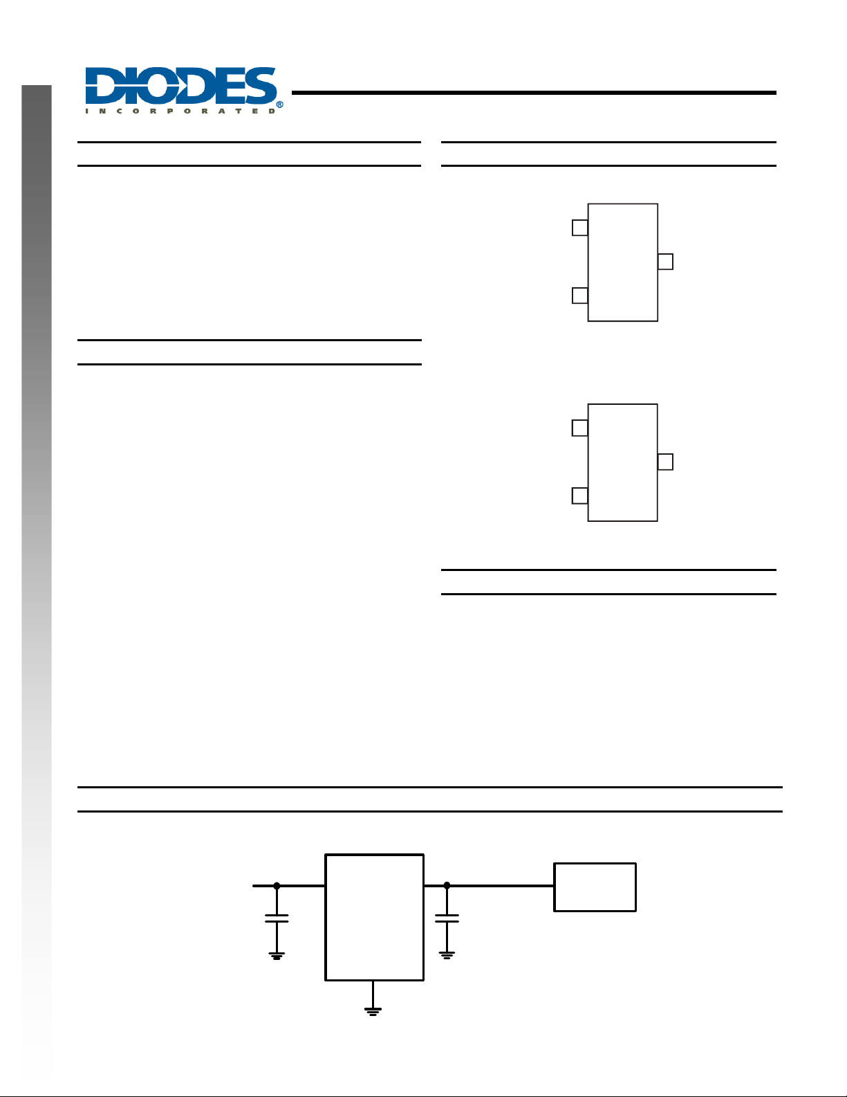
Typical Application Circuit
0.2A SINGLE CHANNEL CURRENT-LIMITED LOAD SWITCH
Pin Assignments
(Top View)
GND
IN
OUT
SOT23
(Top View)
GND
IN
OUT
SC59
Applications
• LCD TVs & Monitors
• Set-Top-Boxes, Residential Gateways
• Laptops, Desktops, Servers
• Printers, Docking Stations, HUBs
• Smart phones, e-Readers
Power Supply
2.7V to 5.2V
AP2331
Document Number: DS35529 Rev. 4 - 2
0.1µF
IN
OUT
GND
1 of 11
www.diodes.com
0.1µF
Load
May 2012
© Diodes Incorporated
Page 2
AP2331
0.2A SINGLE CHANNEL CURRENT-LIMITED LOAD SWITCH
Pin Descriptions
Pin Name Pin Number Descriptions
GND 1 GND
OUT
IN
2 Switch output pin
3 Voltage input pin
Absolute Maximum Ratings
Symbol Parameter Ratings Units
ESD HBM Human Body Model ESD Protection 3 KV
ESD MM Machine Model ESD Protection 300 V
VIN
NEW PRODUCT
Note: 4. UL Recognized Rating from -30°C to +70°C (Diodes qualified TST from -65°C to +150°C)
V
I
LOAD
T
TST
OUT
JMAX
Input Voltage relative to GND 6.5 V
Output Voltage relative to GND
Maximum Continuous Load Current Internal Limited A
Maximum Junction Temperature 150 °C
Storage Temperature Range (Note 4) -65 to +150 °C
Recommended Operating Conditions
Symbol Parameter Min Max Units
V
I
OUT
T
IN
A
Input voltage relative to GND 2.7 5.2 V
Output Current 0 0.2 A
Operating Ambient Temperature -40 +85 °C
AP2331
Document Number: DS35529 Rev. 4 - 2
2 of 11
www.diodes.com
VIN +0.3
V
May 2012
© Diodes Incorporated
Page 3
0.2A SINGLE CHANNEL CURRENT-LIMITED LOAD SWITCH
Electrical Characteristics (T
= 25°C, V
A
Symbol Parameter Test Conditions (Note 5) Min Typ. Max Unit
V
Input UVLO
UVLO
I
Input quiescent current
Q
I
Reverse leakage current
REV
R
I
I
T
V
T
NEW PRODUCT
V
T
T
Notes: 5. Pulse-testing techniques maintain junction temperature close to ambient temperature; thermal effects must be taken into account separately.
6. When reverse current triggers at I
turned off.
8. Since the output turn-on slew rate is dependent on input supply slew rate, this limit is only applicable for input supply slew rate between V
V
Switch on-resistance
DS(ON)
Over-load current limit
LIMIT
IOS
Short-circuit current OUT shorted to ground 0.3 0.4 0.5 A
Reverse-current trigger point
ROCP
Deglitch time from reverse current trigger
TRIG
to MOSFET turn off
Output over-voltage trip point (Note 7) 5.3 5.6 V
OVP
Debounce time from output over-voltage
OVP
to MOSFET turn off
Recovery after turn-off from ROCP and
REC
OVP
TON
Output turn-on time (Note 8)
Thermal shutdown threshold
SHDN
Thermal shutdown hysteresis 20 °C
HYS
Thermal Resistance Junction-to-Ambient
θ
JA
(Note 9)
= 0.20A, the reverse current is continuously clamped at I
ROCP
7. During output over-voltage protection, the output draws approximately 60µA current.
/1ms.
IN
9. Device mounted on FR-4 substrate PCB, 2oz copper, with minimum recommended pad layout.
= +5.0V, unless otherwise stated.)
IN
VIN rising
Above UVLO, I
VIN = 0V, V
V
= 5V, I
IN
VIN = 5V, V
VIN = 5.0V, V
(Note 6) 0.5 0.7 1.0 ms
15 µs
101%
C
L
(UVLO to 90% V
V
SOT23 215
SC59 255
OUT
= 0.1µF, R
= 2.7V to 5.2V
IN
OUT
= 0.2A
OUT
OUT
LOAD
= 0
OUT
= 5V, I
= 4V
= 5.2V
= 20Ω
OUT-NOM
REV
at VIN
)
2.35 2.65 V
85 125 µA
0.01 0.10 µA
100 250 350 mΩ
0.3 0.4 0.5 A
0.20 0.25 A
0.7 ms
150 °C
for 0.7ms deglitch time until MOSFET is
ROCP
AP2331
Document Number: DS35529 Rev. 4 - 2
3 of 11
www.diodes.com
AP2331
VIN
o
C/W
o
C/W
/0.2ms to
IN
May 2012
© Diodes Incorporated
Page 4

A
0.2A SINGLE CHANNEL CURRENT-LIMITED LOAD SWITCH
Typical Performance Characteristics
UVLO Increasing
AP2331
UVLO Decreasing
NEW PRODUCT
1ms/div
Over-Load Current Limit
5ms/div
Deglitch Time from Reverse-Current Trigger to
MOSFET Turn-Off
5ms/div
Short-Circuit Current Limit
100µs/div
Reverse-Current Limit
550µs
200m
200µs/div
AP2331
Document Number: DS35529 Rev. 4 - 2
4 of 11
www.diodes.com
200µs/div
© Diodes Incorporated
May 2012
Page 5

HOR
T CIRCUIT CUR
REN
T
OUTPU
T
TUR
N
O
N
T
O
N
TATE R
TAN
C
0.2A SINGLE CHANNEL CURRENT-LIMITED LOAD SWITCH
Typical Performance Characteristics (cont.)
Output Over-Voltage Trip Point
AP2331
Output Turn-On Time
NEW PRODUCT
OVP at 5.4V
OVP recovery
at 5.1V
10ms/div
140
120
V = 5.2V
100
IN
80
60
40
SUPPLY CURRENT (µA)
V = 3.3V
20
0
-40 -20 0 20 40 60 80
AMBIENT TEMPERATURE ( C)
Fig. 1 Quiescent Supply Current vs.
Ambient Temperature
V = 5V
IN
V = 2.7V
IN
IN
CL=0.1µF
Rload=20Ω
200µs/div
0.408
0.406
0.404
(mA)
0.402
V = 3.3V
IN
0.400
0.398
0.396
0.394
0.392
S
0.390
0.388
°
C = 10µF
L
-40 -20 0 20 40 60 80
AMBIENT TEMPERATURE ( C)
Fig. 2 Sho r t C i r c uit Curr e nt Limit vs .
Ambient Temperature
V = 2.7V
IN
V = 5V,
IN
V = 5.2V
IN
°
0.45
0.40
IME (ms)
-
0.35
0.30
0.25
0.20
2.5 3.0 3.5 4.0 4.5 5.0 5.5
INPUT VOLTAGE (V)
Fig. 3 Output Turn On-Time vs. Input Voltage
C = 1µF
L
R = 5
Ω
L
500
V = 2.7V
IN
Ω
E (m )
450
400
350
V = 3.3V
IN
300
250
ESIS
200
V = 5V
IN
-S
150
100
V = 5.5V
IN
50
0
-40 -20 0 20 40 60 80
AMBIENT TEMPERATURE ( C)
Fig. 4 Switch On-Resistance vs.
Ambient Temperatur e
°
AP2331
Document Number: DS35529 Rev. 4 - 2
5 of 11
www.diodes.com
May 2012
© Diodes Incorporated
Page 6

U
P
PLY CUR
R
T
R
R
CUR
RENT
T
0.2A SINGLE CHANNEL CURRENT-LIMITED LOAD SWITCH
Typical Performance Characteristics (cont.)
NEW PRODUCT
0.402
0.400
0.398
(µA)
EN
0.396
0.394
0.392
S
0.390
0.388
-40 -20 0 20 40 60 80
AMBIENT TEMPERATURE ( C)
Fig. 5 Current Limit Trip Threshold vs.
Ambient Temperat ur e
AP2331
500
450
400
(mA)
350
LIMI
300
250
200
SE
150
100
EVE
50
0
-40 -20 0 20 40
°
V = 3.3V
IN
AMBIENT TEMPERATURE ( C)
Fig. 6 Reverse Current Limit vs .
Ambient Temperat ure
V = 5V
IN
V = 2.7V
IN
60 80
°
AP2331
Document Number: DS35529 Rev. 4 - 2
6 of 11
www.diodes.com
May 2012
© Diodes Incorporated
Page 7

Application information
AP2331
0.2A SINGLE CHANNEL CURRENT-LIMITED LOAD SWITCH
Under-Voltage Lockout (UVLO)
Under-voltage lockout function (UVLO) guarantees that the
internal power switch is initially off during start-up. The UVLO
functions only when the power supply has reached at least 2.5V
(TYP). Whenever the input voltage falls below approximately
2.5V, the power switch is turned off. This facilitates the design of
hot-insertion systems where it is not possible to turn off the power
switch before input power is removed.
S.NO Conditions Explanation Behavior of the AP2331
Output is shorted before input
voltage is applied or before
the part is powered up.
Short-Circuit or Overload
condition that occurs when
the part is powered up and
above UVLO.
Load increases gradually until
the current-limit threshold.
NEW PRODUCT
1 Short-circuit condition at start-up
Short-circuit or Over current
2
condition
Gradual increase from nominal
3
operating current to I
LIMIT
Reverse-Current Protection
The USB specification does not allow an output device to source
current back into the USB port. In a normal MOSFET switch,
current will flow in reverse direction (from the output side to the
input side) when the output side voltage is higher than the input
side. A reverse current limit feature is implemented in the AP2331
to limit such back currents. Reverse current limit is always active
in AP2331. Reverse current is limited at IROCP level and when
the fault exists for more than 700µs, output device is disabled and
shutdown. This is called the "Deglitch time from reverse current
trigger to MOSFET turn off”. Recovery from IROCP occurs when
the output voltage falls to 101% of input voltage.
Over-Voltage Protection
The device has an output over-voltage protection that triggers
when the output voltage reaches 5.3V(MIN). When this fault
condition stays on for longer than 15µs, (This is called the
“Debounce time from output over-voltage to MOSFET turn off”)
output device is disabled and shutdown. Recovery from ROVP
occurs when the output voltage falls to 101% of input voltage.
Thermal Protection
Thermal protection prevents the IC from damage when the die
temperature exceeds safe margins. This mainly occurs when
heavy-overload or short-circuit faults are present for extended
periods of time. The AP2331 implements a thermal sensing to
monitor the operating junction temperature of the power
distribution switch. Once the die temperature rises to
approximately +150°C, the Thermal protection feature gets
activated as follows: The internal thermal sense circuitry turns the
Over-Current and Short-Circuit Protection
An internal sensing FET is employed to check for over current
conditions. Unlike current-sense resistors, sense FETs do not
increase the series resistance of the current path. When an over
current condition is detected, the device maintains a constant
output current and reduces the output voltage accordingly.
Complete shutdown occurs only if the fault stays long enough to
activate thermal limiting.
The different overload conditions and the corresponding response
of the AP2331 are outlined below:
The IC senses the short circuit and immediately clamps
output current to a certain safe level namely I
• At the instance the overload occurs, higher current may
flow for a very short period of time before the current limit
function can react.
• After the current limit function has tripped (reached the
over-current trip threshold), the device switches into
current limiting mode and the current is clamped at I
The current rises until I
reached, the device switches into its current limiting mode
and is clamped at I
power switch off thus preventing the power switch from damage.
Hysteresis in the thermal sense circuit allows the device to cool
down to approximately +20°C before the output is turned back on.
This built-in thermal hysteresis feature is an excellent feature, as it
avoids undesirable oscillations of the thermal protection circuit.
The switch continues to cycle in this manner until the load fault is
removed, resulting in a pulsed output.
LIMIT
. Once the threshold has been
LIMIT
.
LIMIT
.
LIMIT
Discharge Function
When input voltage falls below UVLO, the discharge function is
active. The output capacitor is discharged through an internal
NMOS that has a discharge resistance of 800Ω. Hence, the output
voltage drops down to zero. The time taken for discharge is
dependent on the RC time constant of the resistance and the
output capacitor. Discharge time is calculated when UVLO falling
threshold is reached to output voltage reaching 300mV.
Power Dissipation and Junction Temperature
The low on-resistance of the internal MOSFET allows the small
surface-mount packages to pass large current. Using the
maximum operating ambient temperature (T
power dissipation can be calculated by:
P
= R
D
Finally, calculate the junction temperature:
= PD x R
T
J
Where:
T
= Ambient temperature °C
A
R
= Thermal resistance
JA
θ
P
= Total power dissipation
D
DS(ON)
JA
θ
× I
+ TA
) and R
A
2
DS(ON)
, the
AP2331
Document Number: DS35529 Rev. 4 - 2
7 of 11
www.diodes.com
May 2012
© Diodes Incorporated
Page 8

Ordering Information (cont.)
AP2331
0.2A SINGLE CHANNEL CURRENT-LIMITED LOAD SWITCH
AP 2331 X - 7
Package
SA : SOT23
Packing
7 : Tape & R eel
W : SC59
Device Package Code
AP2331SA-7 SA SOT23 3000/Tape & Reel -7
AP2331W-7 W SC59 3000/Tape & Reel -7
Note: 10. Pad layout as shown on Diodes Inc. suggested pad layout document AP02001, which can be found on our website at
http://www.diodes.com/datasheets/ap02001.pdf.
Packaging
(Note 10)
Quantity Part Number Suffix
Marking Information
NEW PRODUCT
(1) SOT23
7” Tape and Reel
SC59
(2)
AP2331
Document Number: DS35529 Rev. 4 - 2
Device Package Identification Code
AP2331SA-7 SOT23 KJ
( Top View )
XX
3
Y W
XX : Identification code
X
: Year 0~9
Y
W
: Week : A~Z : 1~26 week;
a~z : 27~52 week; z represents
52 and 53 week
: A~Z : Internal code
1 2
X
Device Package Identification Code
AP2331W-7 SC59 KN
8 of 11
www.diodes.com
May 2012
© Diodes Incorporated
Page 9

AP2331
Package Information (All Dimensions in mm)
Package Type:
(1) SOT23
NEW PRODUCT
(2) SC59
K
J
K
J
A
H
F
D
G
A
G
H
D
0.2A SINGLE CHANNEL CURRENT-LIMITED LOAD SWITCH
C
B
K1
L
C
B
N
L
M
M
Dim Min Max Typ
A 0.37 0.51 0.40
B 1.20 1.40 1.30
C 2.30 2.50 2.40
D 0.89 1.03 0.915
F 0.45 0.60 0.535
G 1.78 2.05 1.83
H 2.80 3.00 2.90
J 0.013 0.10 0.05
K 0.903 1.10 1.00
K1 - - 0.400
L 0.45 0.61 0.55
M 0.085 0.18 0.11
α
Dim Min Max Typ
A 0.35 0.50 0.38
B
C
D
G
H
J
K
L
M
N 0.70 0.80 0.75
α
All Dimensions in mm
SOT23
0° 8° -
All Dimensions in mm
SC59
1.50 1.70 1.60
2.70 3.00 2.80
- - 0.95
- - 1.90
2.90 3.10 3.00
0.013 0.10 0.05
1.00 1.30 1.10
0.35 0.55 0.40
0.10 0.20 0.15
0° 8° -
AP2331
Document Number: DS35529 Rev. 4 - 2
9 of 11
www.diodes.com
May 2012
© Diodes Incorporated
Page 10

Suggested Pad Layout
(1) SOT23
Z
Z
NEW PRODUCT
(2) SC59
AP2331
0.2A SINGLE CHANNEL CURRENT-LIMITED LOAD SWITCH
Y
C
X
Y
X E
E
C
Dimensions Value (in mm)
Z 2.9
X 0.8
Y 0.9
C
E
Dimensions Value (in mm)
Z 3.4
X 0.8
Y 1.0
C
E
2.0
1.35
2.4
1.35
AP2331
Document Number: DS35529 Rev. 4 - 2
10 of 11
www.diodes.com
May 2012
© Diodes Incorporated
Page 11

AP2331
0.2A SINGLE CHANNEL CURRENT-LIMITED LOAD SWITCH
NEW PRODUCT
IMPORTANT NOTICE
DIODES INCORPORATED MAKES NO WARRANTY OF ANY KIND, EXPRESS OR IMPLIED, WITH REGARDS TO THIS
DOCUMENT, INCLUDING, BUT NOT LIMITED TO, THE IMPLIED WARRANTIES OF MERCHANTABILITY AND FITNESS FOR A
PARTICULAR PURPOSE (AND THEIR EQUIVALENTS UNDER THE LAWS OF ANY JURISDICTION).
Diodes Incorporated and its subsidiaries reserve the right to make modifications, enhancements, improvements, corrections or other
changes without further notice to this document and any product described herein. Diodes Incorporated does not assume any liability
arising out of the application or use of this document or any product described herein; neither does Diodes Incorporated convey any
license under its patent or trademark rights, nor the rights of others. Any Customer or user of this document or products described
herein in such applications shall assume all risks of such use and will agree to hold Diodes Incorporated and all the companies
whose products are represented on Diodes Incorporated website, harmless against all damages.
Diodes Incorporated does not warrant or accept any liability whatsoever in respect of any products purchased through unauthorized
sales channel.
Should Customers purchase or use Diodes Incorporated products for any unintended or unauthorized application, Customers shall
indemnify and hold Diodes Incorporated and its representatives harmless against all claims, damages, expenses, and attorney fees
arising out of, directly or indirectly, any claim of personal injury or death associated with such unintended or unauthorized application.
Products described herein may be covered by one or more United States, international or foreign patents pending. Product names
and markings noted herein may also be covered by one or more United States, international or foreign trademarks.
LIFE SUPPORT
Diodes Incorporated products are specifically not authorized for use as critical components in life support devices or systems without
the express written approval of the Chief Executive Officer of Diodes Incorporated. As used herein:
A. Life support devices or systems are devices or systems which:
1. are intended to implant into the body, or
2. support or sustain life and whose failure to perform when properly used in accordance with instructions for use provided
in the labeling can be reasonably expected to result in significant injury to the user.
B. A critical component is any component in a life support device or system whose failure to perform can be reasonably expected
to cause the failure of the life support device or to affect its safety or effectiveness.
Customers represent that they have all necessary expertise in the safety and regulatory ramifications of their life support devices or
systems, and acknowledge and agree that they are solely responsible for all legal, regulatory and safety-related requirements
concerning their products and any use of Diodes Incorporated products in such safety-critical, life support devices or systems,
notwithstanding any devices- or systems-related information or support that may be provided by Diodes Incorporated. Further,
Customers must fully indemnify Diodes Incorporated and its representatives against any damages arising out of the use of Diodes
Incorporated products in such safety-critical, life support devices or systems.
Copyright © 2012, Diodes Incorporated
www.diodes.com
AP2331
Document Number: DS35529 Rev. 4 - 2
11 of 11
www.diodes.com
May 2012
© Diodes Incorporated
 Loading...