

Page 1
Data Sheet
600mA LOW DROPOUT LINEAR REGULATOR AP1117M
600mA ULDO REGULATOR WITH ENABLE AP2318
General Description
The AP2318 is a series of ultra low dropout regulators
optimized for low voltage applications where transient
response and minimum input voltage are critical.
The AP2318 provides current limit and thermal
shutdown. Its circuit includes a trimmed bandgap
reference to assure output voltage accuracy to be
within ±1.5%. On-chip thermal shutdown provides
protection against any combination of overload and
ambient temperatures that would create excessive
junction temperatures.
The AP2318 has both fixed and adjustable versions.
The 1.3V fixed versions integrate the corresponding
resistor divider. The adjustable version can set the
output voltage through two external resistors.
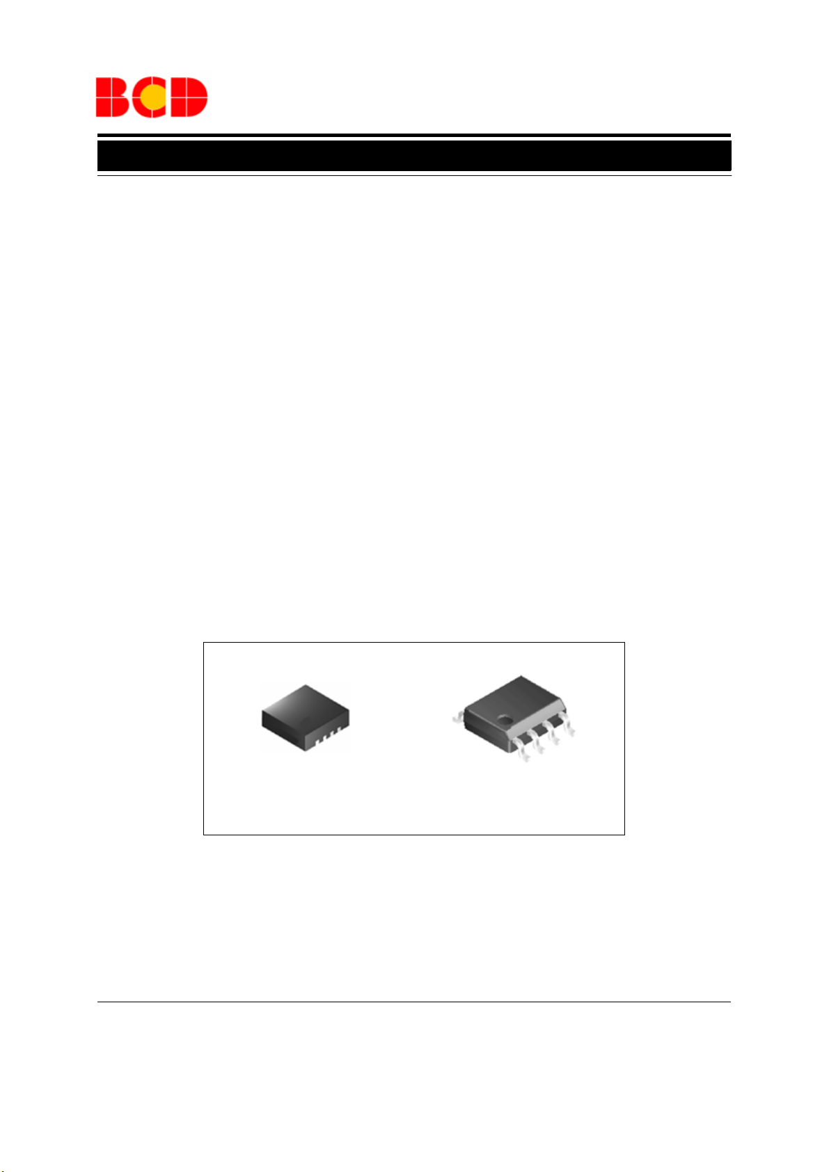
The AP2318 is available in the standard DFN-3×3-8
and SOIC-8 packages.
Features
· Wide Operating Voltage Ranges: 2.5V to 12V
· Output Voltage Accuracy: ±1.5%
· On-chip Thermal Shutdown
· ESD: Human Body Model 3kV
Machine Model 600V
· Operating Junction Temperature: -40oC to 125oC
Applications
· Notebook
· USB Device
· Add-on Card
· DVD Player
· PC Motherboard
DFN-3×3-8
Figure 1. Package Types of AP2318
May. 2011 Rev. 2. 0 BCD Semiconductor Manufacturing Limited
1
SOIC-8
Page 2
Data Sheet
600mA LOW DROPOUT LINEAR REGULATOR AP1117M
600mA ULDO REGULATOR WITH ENABLE AP2318
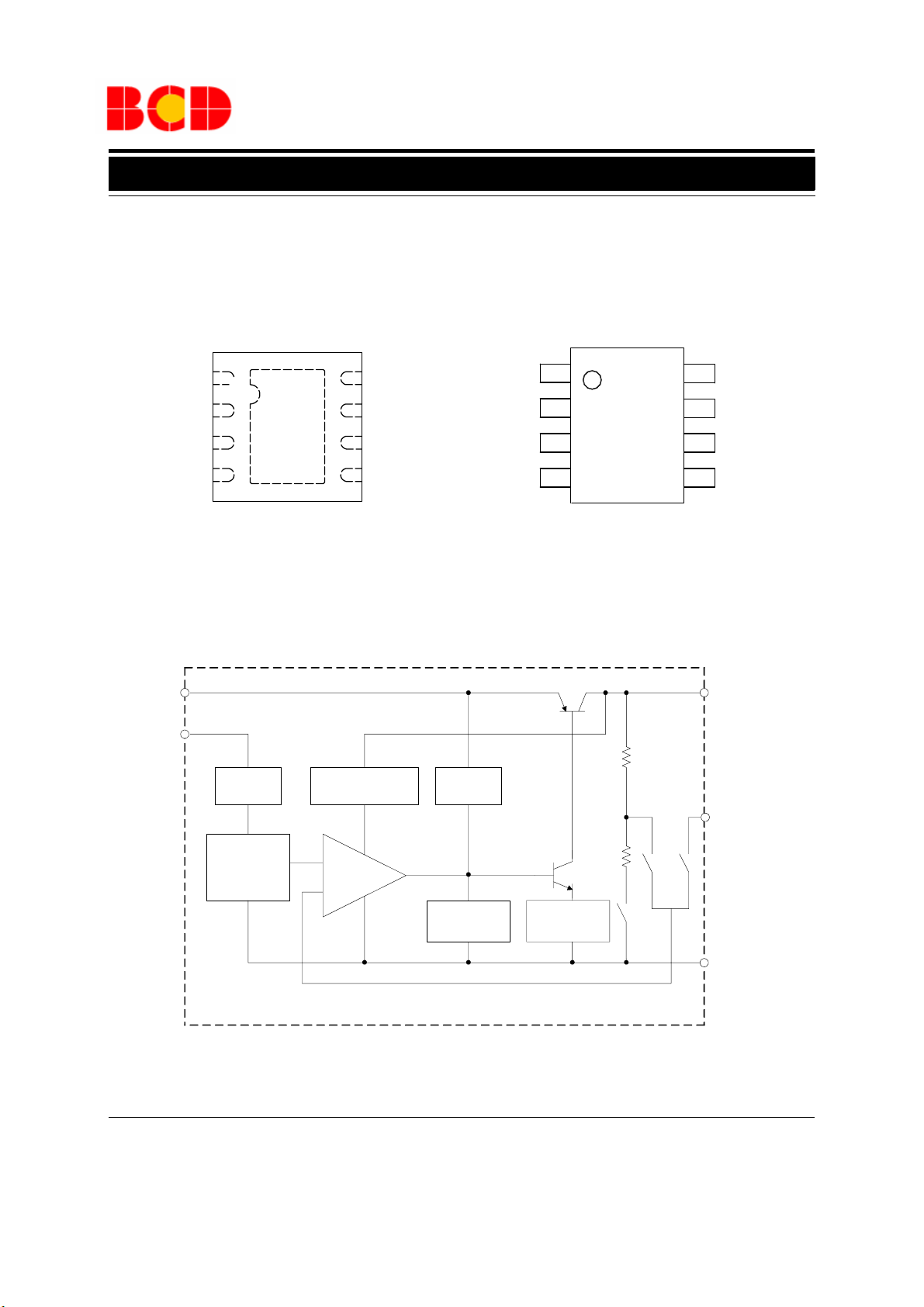
Pin Configuration
DN Package
(DFN-3x3-8)
V
1
IN
V
2
IN
V
OUT
3
V
45
OUT
Figure 2. Pin Configuration of AP2318 (Top View)
Functional Block Diagram
1, 2 (3, 4)
V
IN
8
7
6
EN
NC
GND
ADJ/NC
NC
EN
V
V
M Package
(SOIC-8)
8
7
6
5
GND
ADJ/NC
V
OUT
NC
V
OUT
1
2
3
IN
4
IN
3, 4 (6)
8 (2)
EN
Enable
Bandgap
Reference
V
RC
Compensation
Error
FB
Amplifier
OVP
Thermal
Shutdown
Current
Limit
A2
A1
5 (7)
6 (8)
ADJ/NC
B
GND
Connect A1 and A2, disconnect B: Fixed Voltage Version
Connect B, disconnect A1 and A2:Adjustable Voltage Version
A (B)
A: DFN-3x3-8
B: SOIC-8
Figure 3. Functional Block Diagram of AP2318
May. 2011 Rev. 2. 0 BCD Semiconductor Manufacturing Limited
2
Page 3
Data Sheet
600mA LOW DROPOUT LINEAR REGULATOR AP1117M
600mA ULDO REGULATOR WITH ENABLE AP2318
Pin Description
Pin Number
×3-8
DFN-3
1, 2 3, 4
3, 4 6
SOIC-8
Pin Name Function
V
V
OUT
IN
Input Voltage
Output Voltage
5 7 ADJ/NC Adjust Voltage/No Connection
6 8 GND Ground
7 1, 5 NC No connection
8 2 EN On/Off control
Ordering Information
AP2318 -
Circuit Type
Package
M: SOIC-8
DN: DFN-3×3-8
E1: Lead Free
G1: Green
TR: Tape and Reel
Blank: Tube
ADJ: Adjustable Output
1.3: Fixed Output 1.3V
Package
SOIC-8
DFN-3
×3-8
Te mp er at ur e
Range
-40 to
125oC
-40 to
125oC
Part Number Marking ID
Lead Free Green Lead Free Green
AP2318M-ADJE1 AP2318M-ADJG1 2318M-ADJE1 2318M-ADJG1 Tube
AP2318M-ADJTRE1 AP2318M-ADJTRG1 2318M-ADJE1 2318M-ADJG1 Tape & Reel
AP2318M-1.3E1 AP2318M-1.3G1 2318M-1.3E1 2318M-1.3G1 Tube
AP2318M-1.3TRE1 AP2318M-1.3TRG1 2318M-1.3E1 2318M-1.3G1 Tape & Reel
AP2318DN-ADJTRE1 AP2318DN-ADJTRG1 F9E B9E
AP2318DN-1.3TRE1 AP2318DN-1.3TRG1 F9B B9B
Packing
Typ e
Tap e & Reel
Tap e & Reel
BCD Semiconductor's Pb-free products, as designated with "E1" suffix in the part number, are RoHS compliant. Products with
"G1" suffix are available in green packages.
May. 2011 Rev. 2. 0 BCD Semiconductor Manufacturing Limited
3
Page 4
Data Sheet
600mA LOW DROPOUT LINEAR REGULATOR AP1117M
600mA ULDO REGULATOR WITH ENABLE AP2318
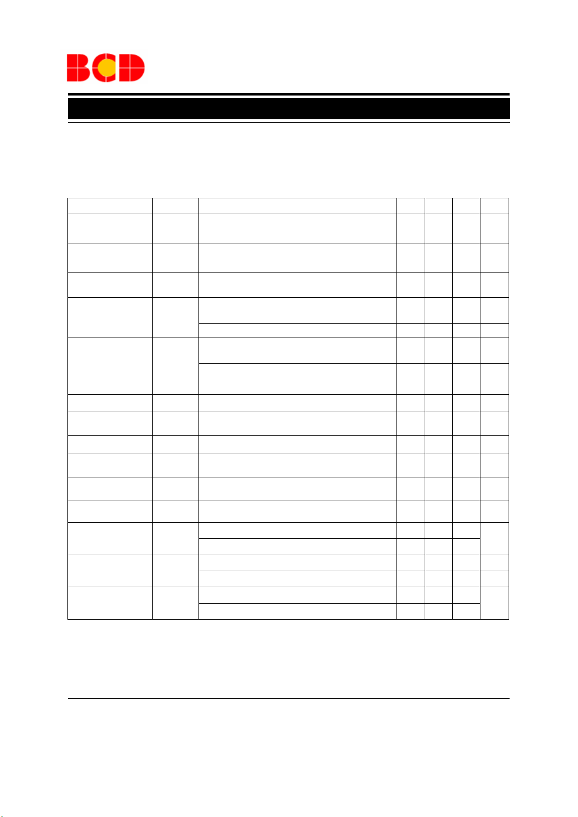
Absolute Maximum Ratings (Note 1)
Parameter Symbol Value Unit
Input Voltage V
Operating Junction Temperature T
Storage Temperature Range T
Lead Temperature (Soldering, 10sec) T
LEAD
Thermal Resistance (Note 2) θ
IN
J
STG
SOIC-8 135
JA
15 V
150
-65 to 150
260
o
C/W
o
C
o
C
o
C
DFN-3×3-8 120
ESD (Human Body Model) ESD 3000 V
ESD (Machine Model) ESD 600 V
Note 1: Stresses greater than those listed under "Absolute Maximum Ratings" may cause permanent damage to the device.
These are stress ratings only, and functional operation of the device at these or any other conditions beyond those indicated
under "Recommended Operating Conditions" is not implied. Exposure to "Absolute Maximum Ratings" for extended periods
may affect device reliability.
Note 2: Absolute maximum ratings indicate limits beyond which damage to the component may occur. Electrical specifications do not apply when operating the device outside of its operating ratings. The maximum allowable power dissipation is a
function of the maximum junction temperature, T
perature, T
)/θ
T
A
The maximum allowable power dissipation at any ambient temperature is calculated using: PD(max)=(TJ(max) -
A.
Exceeding the maximum allowable power dissipation will result in excessive die temperature, and the regulator will
JA.
(max), the junction-to-ambient thermal resistance,θ
J
and the ambient tem-
JA,
go into thermal shutdown.
Recommended Operating Conditions
Parameter Symbol Min Max Unit
Input Voltage
Enable Voltage
Operating Junction Temperature Range T
V
V
IN
EN
J
May. 2011 Rev. 2. 0 BCD Semiconductor Manufacturing Limited
4
2.5 12 V
12 V
-40 125
o
C
Page 5
Data Sheet
600mA LOW DROPOUT LINEAR REGULATOR AP1117M
600mA ULDO REGULATOR WITH ENABLE AP2318
Electrical Characteristics
Operating Conditions: 2.5V≤V
≤12V, CIN=1µF, C
IN
=2.2µF, TJ=25oC, unless otherwise specified. (P≤Maxi-
OUT
mum Power Dissipation). Limits appearing in Boldface type apply over the entire junction temperature range for
operation of -40
Parameter
Reference Voltage
Output Voltage
Maximum Output
Current
Line Regulation
Load Regulation
Dropout Voltage
Adjust Pin Current
Minimum Load
Current
Quiescent Current
RMS Output Noise
(% of V
OUT
Thermal Shutdown
Temperature
Thermal Shutdown
Hysteresis
Enable Input Voltage
Enable Input Current
Thermal Resistance,
(Junction to Case)
o
)
C to 125oC.
Symbol
V
V
I
OUT
V
RLINE
V
RLOAD
V
DROP
I
ADJ
I
LOAD
I
V
V
I
θ
REF
OUT
AP2318-ADJ I
10mA≤I
I
OUT
10mA≤I
(max) VIN-V
AP2318-ADJ
I
OUT
I
OUT
AP2318-ADJ
V
IN=VOUT
V
IN
∆V
OUT
(min) V
Q
NOI
OUT
VIN=V
TA=25oC, 10Hz≤f≤20kHz
Enable logic low 0.8
EN
Enable logic high 2.25
VEN=2.25V
EN
V
EN
DFN-3×3-8
JC
SOIC-8 24
Conditions
=10mA, VIN-V
OUT
≤600mA, V
OUT
+2V≤VIN ≤12V
OUT
=10mA, VIN=2.5V, TJ=25oC
≤600mA, 2.5V≤VIN ≤12V
OUT
=2V
OUT
=10mA, V
+2V≤VIN≤12V
OUT
=2V, TJ=25oC
OUT
Min Typ Max Unit
0.788
0.800
0.812
0.784
0.800
0.816
-1.5%
-2%
1.5%
2%
0.85 1.2 A
1 6 mV
=10mA, 2.5V≤VIN ≤12V 1 6 mV
+2V, 10mA≤I
=2.5V, 10mA≤I
(∆V
)=1%, I
REF
≤600mA
OUT
≤600mA 1 10 mV
OUT
=600mA
OUT
1 10 mV
0.35 V
0.05 1
+2V≤VIN≤12V (ADJ only)
OUT
+2V, I
OUT
=0mA
1.7 5 mA
250
0.003 %
150
25
515µA
=0.8V
15
4 µA
o
V
V
µA
µA
o
C
o
C
V
C/W
May. 2011 Rev. 2. 0 BCD Semiconductor Manufacturing Limited
5
Page 6

Data Sheet
600mA LOW DROPOUT LINEAR REGULATOR AP1117M
600mA ULDO REGULATOR WITH ENABLE AP2318
Typical Performance Characteristics
0.90
0.88
0.86
0.84
0.82
0.80
0.78
Output Voltage (V)
0.76
0.74
0.72
0.70
0 50 100 150 200 250 300
AP2318-ADJ
V
OUT
ADJ short to GND
T
=25oC
C
VIN=2.8V
Output Current (mA)
Figure 4. Output Voltage vs. Output Current
(Conditions: V
1.0
0.9
0.8
0.7
0.6
0.5
0.4
Output Voltage (V)
0.3
0.2
0.1
0.0
0 150 300 450 600 750 900 1050 1200 1350 1500
=0.8V, ADJ Short to GND)
OUT
AP2318-ADJ
V
OUT
ADJ short to GND
=25oC
T
C
Output Current (mA)
=0.8V
VIN=3.2V
VIN=8V
VIN=12V
=0.8V
1.30
1.28
1.26
1.24
1.22
1.20
1.18
Output Voltage (V)
1.16
1.14
1.12
1.10
0 50 100 150 200 250 300
AP2318-ADJ
V
OUT
R1=3k
R2=6.2kΩ
TC=25oC
VIN=3.2V
Output Current (mA)
Figure 5. Output Voltage vs. Output Current
(Conditions: V
1.5
1.4
1.3
1.2
1.1
1.0
0.9
0.8
0.7
0.6
0.5
Output Voltage (V)
0.4
0.3
0.2
0.1
0.0
0 150 300 450 600 750 900 1050 1200 1350 1500
=1.2V, R1=3kΩ, R2=6.2kΩ)
OUT
Output Current (mA)
AP2318-ADJ
V
OUT
R1=3k
R2=6.2kΩ
TC=25oC
VIN=3.2V
VIN=2.5V
VIN=12V
=1.2V
Ω
=1.2V
Ω
Figure 6. Output Voltage vs. Output Current
(Conditions: V
=0.8V, ADJ Short to GND)
OUT
Figure 7. Output Voltage vs. Output Current
(Conditions: V
=1.2V, R1=3kΩ, R2=6.2kΩ)
OUT
May. 2011 Rev. 2. 0 BCD Semiconductor Manufacturing Limited
6
Page 7

Data Sheet
600mA LOW DROPOUT LINEAR REGULATOR AP1117M
600mA ULDO REGULATOR WITH ENABLE AP2318
Typical Performance Characteristics (Continued)
1.1
1.0
0.9
0.8
0.7
0.6
0.5
0.4
Output Voltage (V)
0.3
0.2
0.1
0.0
0 150 300 450 600 750 900 1050 1200 1 350 1500
AP2318-ADJ
V
=2.8V
IN
=0.8V
V
OUT
ADJ short to GND
TC=25oC
TC=-40oC
TC=125oC
Output Current (mA)
Figure 8. Output Voltage vs. Output Current
(Conditions: V
1.0
0.9
0.8
0.7
0.6
0.5
0.4
0.3
Output Voltage (V)
0.2
0.1
0.0
0123456789101112
=0.8V, ADJ Short to GND)
OUT
AP2318-ADJ
=0.8V
V
OUT
ADJ short to GND
T
=25oC
C
300mA
10mA
600mA
Input Voltage (V)
1.5
1.4
1.3
1.2
1.1
1.0
0.9
0.8
0.7
0.6
0.5
Output Voltage (V)
0.4
0.3
0.2
0.1
0.0
0 150 300 450 600 750 900 1050 1200 1350 1500
AP2318-ADJ
V
=3.2V
IN
V
=1.2V
OUT
R1=3k
Ω
R2=6.2kΩ
TC=25oC
TC=-40oC
TC=125oC
Output Current (mA)
Figure 9. Output Voltage vs. Output Current
(Conditions: V
1.4
1.2
1.0
0.8
0.6
Output Voltage (V)
0.4
0.2
0.0
0123456789101112
=1.2V, R1=3kΩ, R2=6.2kΩ)
OUT
AP2318-ADJ
=1.2V
V
OUT
R1=3k
R2=6.2kΩ
TC=25oC
300mA
10mA
600mA
Input Voltage (V)
Ω
Figure 10. Output Voltage vs. Input Voltage
(Conditions: V
=0.8V, ADJ Short to GND)
OUT
Figure 11. Output Voltage vs. Input Voltage
(Conditions: V
=1.2V, R1=3kΩ, R2=6.2kΩ)
OUT
May. 2011 Rev. 2. 0 BCD Semiconductor Manufacturing Limited
7
Page 8

Data Sheet
600mA LOW DROPOUT LINEAR REGULATOR AP1117M
600mA ULDO REGULATOR WITH ENABLE AP2318
Typical Performance Characteristics (Continued)
0.90
0.88
0.86
0.84
0.82
0.80
0.78
Output Voltage (V)
0.76
0.74
0.72
0.70
-40 -20 0 20 40 60 80 100 120
AP2318-ADJ
=2.8V
V
IN
V
=0.8V
OUT
ADJ short to GND
=10mA
I
OUT
Case Temperature (oC)
Figure 12. Output Voltage vs. Case Temperature
(Conditions: V
250
225
200
175
150
125
100
Supply Current (µA)
75
50
25
0
012345678
=0.8V, ADJ Short to GND)
OUT
Input Voltage (V)
AP2318-ADJ
V
=0.8V
OUT
ADJ short to GND
No Load
TC=-40oC
TC=25oC
TC=125oC
1.30
1.28
1.26
1.24
1.22
1.20
1.18
Output Voltage (V)
1.16
1.14
1.12
1.10
-40-200 20406080100120
AP2318-ADJ
=3.2V
V
IN
V
=1.2V
OUT
Ω
R1=3k
R2=6.2kΩ
I
=10mA
OUT
Case Temperature (oC)
Figure 13. Output Voltage vs. Case Temperature
(Conditions: V
400
350
300
250
200
150
Supply Current (µA)
100
50
0
012345678
=1.2V, R1=3kΩ, R2=6.2kΩ)
OUT
AP2318-ADJ
V
OUT
R1=3k
R2=6.2kΩ
No Load
Input Voltage (V)
=1.2V
Ω
TC=-40oC
TC=25oC
TC=125oC
Figure 14. Supply Voltage vs. Input Voltage
(Conditions: V
=0.8V, ADJ Short to GND)
OUT
Figure 15. Supply Voltage vs. Input Voltage
(Conditions: V
=1.2V, R1=3kΩ, R2=6.2kΩ)
OUT
May. 2011 Rev. 2. 0 BCD Semiconductor Manufacturing Limited
8
Page 9

Data Sheet
600mA LOW DROPOUT LINEAR REGULATOR AP1117M
600mA ULDO REGULATOR WITH ENABLE AP2318
Typical Performance Characteristics (Continued)
220
216
212
208
204
200
196
Supply Current (µA)
192
188
184
180
-40-200 20406080100120
AP2318-ADJ
V
=2.8V
IN
V
=0.8V
OUT
ADJ short to GND
No Load
Case Temperature (oC)
Figure 16. Supply Current vs. Case Temperature
(Conditions: V
20
18
16
14
12
10
8
6
Supply Current (mA)
4
2
0
0 150 300 450 600 750 900 1050 1200 1350 1500
=0.8V, ADJ Short to GND)
OUT
AP2318-ADJ
V
IN
V
OUT
ADJ short to GND
Output Current (mA)
=2.8V
=0.8V
TC=25oC
TC=-40oC
TC=125oC
340
336
332
328
324
320
316
Supply Current (µA)
312
308
304
300
-40-200 20406080100120
AP2318-ADJ
V
=3.2V
IN
V
=1.2V
OUT
R1=3k
Ω
R2=6.2kΩ
No Load
Case Temperature (oC)
Figure 17. Supply current vs. Case Temperature
(Conditions: V
20
18
16
14
12
10
8
6
Supply Current (mA)
4
2
0
0 150 300 450 600 750 900 1050 1200 1350 1500
=1.2V, R1=3kΩ, R2=6.2kΩ)
OUT
AP2318-ADJ
V
IN
V
OUT
R1=3k
R2=6.2kΩ
Output Current (mA)
=3.2V
=1.2V
Ω
TC=25oC
TC=-40oC
TC=125oC
Figure 18. Supply Current vs. Output Current
(Conditions: V
=0.8V, ADJ Short to GND)
OUT
Figure 19. Supply Current vs. Output Current
(Conditions: V
=1.2V, R1=3kΩ, R2=6.2kΩ)
OUT
May. 2011 Rev. 2. 0 BCD Semiconductor Manufacturing Limited
9
Page 10

Data Sheet
600mA LOW DROPOUT LINEAR REGULATOR AP1117M
600mA ULDO REGULATOR WITH ENABLE AP2318
Typical Performance Characteristics (Continued)
20
18
16
14
12
10
8
Supply Current (mA)
6
4
2
0
0 150 300 450 600 750 900 1050 1200 1350 1500
Output Current (mA)
AP2318-ADJ
V
=0.8V
OUT
ADJ short to GND
T
=25oC
C
VIN=3.2V
VIN=8V
VIN=12V
Figure 20. Supply Current vs. Output Current
(Conditions: V
=0.8V, ADJ Short to GND)
OUT
20
18
16
14
12
10
8
Supply Current (mA)
6
4
2
0
0 150 300 450 600 750 900 1050 1200 1 350 1500
Output Current (mA)
AP2318-ADJ
V
=1.2V
OUT
R1=3k
R2=6.2kΩ
TC=25oC
VIN=3.2V
VIN=2.5V
VIN=12V
Figure 21. Supply Current vs. Output Current
(Conditions: V
=1.2V, R1=3kΩ, R2=6.2kΩ)
OUT
Ω
(100mA/Div)
OUT
I
(5 0mV /Di v)
OUT
V
∆
Time (200µs/Div) Time (200µs/Div)
(200mA/Div)
OUT
I
(100mV/Div)
OUT
V
∆
Figure 23. Load Transient ResponseFigure 22. Load Transient Response
(Conditions: V
=2.5V, V
IN
CIN=1µF, C
OUT
=1.3V, I
=2.2µF)
OUT
=1mA to 300mA,
OUT
(Conditions: V
=2.5V, V
IN
C
IN
OUT
=1µF, C
=1.8V, I
=2.2µF)
OUT
=1mA to 600mA,
OUT
May. 2011 Rev. 2. 0 BCD Semiconductor Manufacturing Limited
10
Page 11

Data Sheet
600mA LOW DROPOUT LINEAR REGULATOR AP1117M
600mA ULDO REGULATOR WITH ENABLE AP2318
Typical Performance Characteristics (Continued)
(2V/Div)
OUT
V
∆
(50mV/Div)
IN
V
∆
Figure 24. Line Transient Response
(Conditions: VIN=2.5V to 5V, V
C
=0µF, C
IN
100
90
80
70
60
50
40
PSRR (dB)
AP2318-ADJ
30
V
=1.2V
OUT
V
20
10
0
10 100 1k 10k 100k
IN
C
IN
I
LOAD
=3 to 4V
=1µF, C
=10mA
OUT
=2.2µF
OUT
Frequency (Hz)
=0.8V, I
OUT
=2.2µF)
OUT
=10mA,
(5V/Div)
OUT
V
∆
(50mV/Div)
IN
V
∆
Figure 25. Line Transient Response
(Conditions: V
100
90
80
70
60
50
40
PSRR (dB)
30
20
10
0
10 100 1k 10k 100k
IN
C
AP2318-ADJ
=0.8V
V
OUT
V
=3 to 4V
IN
=1µF, C
C
IN
I
=10mA
LOAD
=2.5V to 10V, V
=0µF, C
IN
OUT
=2.2µF
OUT
Frequency (Hz)
=0.8V, I
OUT
=2.2µF)
OUT
=10mA,
Figure 26. PSRR vs. Frequency
Figure 27. PSRR vs. Frequency
May. 2011 Rev. 2. 0 BCD Semiconductor Manufacturing Limited
11
Page 12

Data Sheet
600mA LOW DROPOUT LINEAR REGULATOR AP1117M
600mA ULDO REGULATOR WITH ENABLE AP2318
Typical Performance Characteristics (Continued)
1.2
1.1
1.0
0.9
0.8
0.7
AP2318-ADJ
0.6
0.5
0.4
0.3
Power Dissipation (W)
0.2
0.1
0.0
=3.2V
V
IN
V
=1.2V
OUT
R1=3k
Ω
R2=6.2kΩ
SOIC-8
=1µF
C
IN
C
=2.2µF
OUT
30 40 50 60 70 80 90 100 110 120
Ambient Temperature (oC)
Figure 28. Power Dissipation vs. Ambient Temperature
(Conditions: V
=1.2V, R1=3kΩ, R2=6.2kΩ)
OUT
1.4
1.2
1.0
0.8
0.6
Output Voltage (V)
0.4
0.2
0.0
0.0 0.5 1.0 1.5 2.0 2.5 3.0 3.5 4.0 4.5 5.0 5.5 6.0
Enable Input Voltage (V)
AP2318-ADJ
V
=1.2V
OUT
V
=3.3V
IN
R1=3k
Ω
R2=6.2kΩ
TC=25oC
I
=10mA
OUT
Figure 29. Output Voltage vs. Enable Input Voltage
(Conditions: V
=1.2V, R1=3kΩ, R2=6.2kΩ)
OUT
May. 2011 Rev. 2. 0 BCD Semiconductor Manufacturing Limited
12
Page 13

Data Sheet
600mA LOW DROPOUT LINEAR REGULATOR AP1117M
600mA ULDO REGULATOR WITH ENABLE AP2318
Typical Applications
V
V
IN
C
IN
1µF
=3.3V
IN
1µF
V
IN
V
AP2318-ADJ
EN
+
GND
Figure 30. Typical Applications of AP2318 ADJ Version, V
V
IN
ADJ/
NC
AP2318-1.3
EN
C
+
IN
GND
OUT
V
OUT
ADJ/
NC
R1
R2
=0.8*(R1+R2)/R2
OUT
+
2.2µF
V
+
V
OUT
C
OUT
OUT
C
2.2µF
=1.3V
OUT
Figure 31. Typical Applications of AP2318 Fixed 1.3V Version, V
OUT
=1.3V
May. 2011 Rev. 2. 0 BCD Semiconductor Manufacturing Limited
13
Page 14

Data Sheet
600mA LOW DROPOUT LINEAR REGULATOR AP1117M
600mA ULDO REGULATOR WITH ENABLE AP2318
Mechanical Dimensions
Unit: mm(inch)SOIC-8
1.000(0.039)
4.700(0.185)
5.100(0.201)
7
°
7
°
1.270(0.050)
TYP
0.100(0.004)
0.300(0.012)
1.350(0.053)
1.750(0.069)
0.675(0.027)
0.725(0.029)
R0.150(0.006)
3.800(0.150)
4.000(0.157)
0.320(0.013)
°
8
°
8
D
2
D
1
:
0
5.800(0.228)
6.200(0.244)
0.800(0.031)
φ
0.200(0.008)
0
°
°
8
0.330(0.013)
0.510(0.020)
0.190(0.007)
0.250(0.010)
0.900(0.035)
1°
5°
0.450(0.017)
0.800(0.031)
)
6
0
0
.
(
0
0
5
1
.
0
R
Note: Eject hole, oriented hole and mold mark is optional.
May. 2011 Rev. 2. 0 BCD Semiconductor Manufacturing Limited
14
Page 15

Data Sheet
600mA LOW DROPOUT LINEAR REGULATOR AP1117M
600mA ULDO REGULATOR WITH ENABLE AP2318
Mechanical Dimensions (Continued)
DFN-3x3-8 Unit: mm(inch)
0.700(0.028)
0.800(0.031)
2.900(0.114)
3.100(0.122)
Pin 1 Dot
by Marking
2.900(0.114)
3.100(0.122)
0.000(0.000)
0.050(0.002)
0.153(0.006)
0.253(0.010)
1.400(0.055)
1.600(0.063)
0.180(0.007)
0.300(0.012)
N5
N4
0
5
6
.
0
)
6
2
0
.
0
(
C
S
B
N8
0.375(0.015)
0.575(0.023)
2.200(0.087)
2.400(0.094)
PIN #1
IDENTIFICATION
N1
May. 2011 Rev. 2. 0 BCD Semiconductor Manufacturing Limited
15
Page 16

BCD Semiconductor Manufacturing Limited
IMPORTANT NOTICE
IMPORTANT NOTICE
BCD Semiconductor Manufacturing Limited reserves the right to make changes without further notice to any products or specifi-
BCD Semiconductor Manufacturing Limited reserves the right to make changes without further notice to any products or specifi-
cations herein. BCD Semiconductor Manufacturing Limited does not assume any responsibility for use of any its products for any
cations herein. BCD Semiconductor Manufacturing Limited does not assume any responsibility for use of any its products for any
particular purpose, nor does BCD Semiconductor Manufacturing Limited assume any liability arising out of the application or use
particular purpose, nor does BCD Semiconductor Manufacturing Limited assume any liability arising out of the application or use
of any its products or circuits. BCD Semiconductor Manufacturing Limited does not convey any license under its patent rights or
of any its products or circuits. BCD Semiconductor Manufacturing Limited does not convey any license under its patent rights or
other rights nor the rights of others.
other rights nor the rights of others.
http://www.bcdsemi.com
MAIN SITE
MAIN SITE
- Headquarters
BCD Semiconductor Manufacturing Limited
BCD Semiconductor Manufactur ing Limited
- Wafer Fab
No. 1600, Zi Xing Road, Shanghai ZiZhu Science-based Industrial Park, 200241, China
Shanghai SIM-BCD Semiconductor Manufacturing Limited
Tel: +86-21-24162266, Fax: +86-21-24162277
800, Yi Shan Road, Shanghai 200233, China
Tel: +86-21-6485 1491, Fax: +86-21-5450 0008
REGIONAL SALES OFFICE
Shenzhen Office
REGIONAL SALES OFFICE
Shanghai SIM-BCD Semiconductor Manufacturing Co., Ltd., Shenzhen Office
Shenzhen Office
Unit A Room 1203, Skyworth Bldg., Gaoxin Ave.1.S., Nanshan District, Shenzhen,
Shanghai SIM-BCD Semiconductor Manufacturing Co., Ltd. Shenzhen Office
China
Advanced Analog Circuits (Shanghai) Corporation Shenzhen Office
Tel: +86-755-8826 7951
Room E, 5F, Noble Center, No.1006, 3rd Fuzhong Road, Futian District, Shenzhen 518026, China
Fax: +86-755-8826 7865
Tel: +86-755-8826 7951
Fax: +86-755-8826 7865
- Wafer Fab
BCD Semiconductor Manufacturing Limited
Shanghai SIM-BCD Semiconductor Manufacturing Co., Ltd.
- IC Design Group
800 Yi Shan Road, Shanghai 200233, China
Advanced Analog Circuits (Shanghai) Corporation
Tel: +86-21-6485 1491, Fax: +86-21-5450 0008
8F, Zone B, 900, Yi Shan Road, Shanghai 200233, China
Tel: +86-21-6495 9539, Fax: +86-21-6485 9673
Taiwan Office
BCD Semiconductor (Taiwan) Company Limited
Taiwan Office
4F, 298-1, Rui Guang Road, Nei-Hu District, Taipei,
BCD Semiconductor (Taiwan) Company Limited
Tai wan
4F, 298-1, Rui Guang Road, Nei-Hu District, Taipei,
Tel: +886-2-2656 2808
Taiwan
Fax: +886-2-2656 2806
Tel: +886-2-2656 2808
Fax: +886-2-2656 2806
USA Office
BCD Semiconductor Corp.
USA Office
30920 Huntwood Ave. Hayward,
BCD Semiconductor Corporation
CA 94544, USA
30920 Huntwood Ave. Hayward,
Tel : +1-510-324-2988
CA 94544, U.S.A
Fax: +1-510-324-2788
Tel : +1-510-324-2988
Fax: +1-510-324-2788
 Loading...